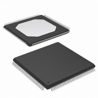
XC3S100E-4TQG144I Xilinx Inc, XC3S100E-4TQG144I Datasheet - Page 122

XC3S100E-4TQG144I
Manufacturer Part Number
XC3S100E-4TQG144I
Description
IC FPGA SPARTAN-3E 100K 144-TQFP
Manufacturer
Xilinx Inc
Series
Spartan™-3Er
Datasheet
1.XC3S100E-4TQG144I.pdf
(193 pages)
Specifications of XC3S100E-4TQG144I
Package / Case
144-TQFP, 144-VQFP
Mounting Type
Surface Mount
Voltage - Supply
1.1 V ~ 3.465 V
Operating Temperature
-40°C ~ 100°C
Number Of I /o
108
Number Of Logic Elements/cells
*
Number Of Gates
*
Lead Free Status / RoHS Status
Lead free / RoHS Compliant
Available stocks
Company
Part Number
Manufacturer
Quantity
Price
Company:
Part Number:
XC3S100E-4TQG144I
Manufacturer:
XILINX/21
Quantity:
163
Company:
Part Number:
XC3S100E-4TQG144I
Manufacturer:
Xilinx Inc
Quantity:
10 000
Part Number:
XC3S100E-4TQG144I
Manufacturer:
XILINX/赛灵思
Quantity:
20 000
DS312-4 (v1.1) March 21, 2005
Introduction
This section describes the various pins on a Spartan™-3E
FPGA and how they connect within the supported compo-
nent packages.
Table 1: Types of Pins on Spartan-3E FPGAs
DS312-4 (v1.1) March 21, 2005
Advance Product Specification
I/O
INPUT
DUAL
VREF
GCLK
LHCLK
RHCLK
CONFIG
Color Code
Type /
© 2005 Xilinx, Inc. All rights reserved. XILINX, the Xilinx logo, and other designated brands included herein are trademarks of Xilinx, Inc.
Unrestricted, general-purpose user-I/O pin. Most pins can be paired together to
form differential I/Os.
Unrestricted, general-purpose input-only pin. This pin does not have an output
structure.
Dual-purpose pin used in some configuration modes during the configuration
process and then usually available as a user I/O after configuration. If the pin is
not used during configuration, this pin behaves as an I/O-type pin. Some of the
dual-purpose pins are also global or edge clock inputs (GCLK).
Dual-purpose pin that is either a user-I/O pin or, along with all other VREF pins
in the same bank, provides a reference voltage input for certain I/O standards.
If used for a reference voltage within a bank, all VREF pins within the bank must
be connected.
Either a user-I/O pin or an input to a specific clock buffer driver. Every package
has 16 global clock inputs that optionally clock the entire device. The RHCLK
inputs optionally clock the right-hand side of the device. The LHCLK inputs
optionally clock the left-hand side of the device. Some of the clock pins are
shared with the dual-purpose configuration pins and are considered DUAL-type.
Dedicated configuration pin. Not available as a user-I/O pin. Every package has
two dedicated configuration pins. These pins are powered by VCCAUX.
R
All other trademarks are the property of their respective owners.
Description
072
0
www.xilinx.com
0
Spartan-3E FPGA Family:
Pinout Descriptions
Advance Product Specification
Pin Types
A majority of the pins on a Spartan-3E FPGA are gen-
eral-purpose, user-defined I/O pins. There are, however, up
to 11 different functional types of pins on Spartan-3E pack-
ages, as outlined in
ings that follow, the individual pins are color-coded
according to pin type as in the table.
Table
1. In the package footprint draw-
IO
IO_Lxxy_#
IP
IP_Lxxy_#
M[2:0]
HSWAP
CCLK
MOSI/CSI_B
D[7:1]
D0/DIN
CSO_B
RDWR_B
BUSY/DOUT
INIT_B
A[23:20]
A19/VS2
A18/VS1
A17/VS0
A[16:0]
LDC[2:0]
HDC
IP/VREF_#
IP_Lxx_#/VREF_#
GCLK[15:0],
LHCLK[7:0],
RHCLK[7:0]
DONE, PROG_B
Pin Name(s) in Type
1


