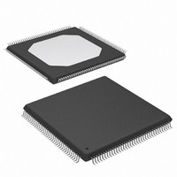
XC3S100E-4TQG144I Xilinx Inc, XC3S100E-4TQG144I Datasheet - Page 37

XC3S100E-4TQG144I
Manufacturer Part Number
XC3S100E-4TQG144I
Description
IC FPGA SPARTAN-3E 100K 144-TQFP
Manufacturer
Xilinx Inc
Series
Spartan™-3Er
Datasheet
1.XC3S100E-4TQG144I.pdf
(193 pages)
Specifications of XC3S100E-4TQG144I
Package / Case
144-TQFP, 144-VQFP
Mounting Type
Surface Mount
Voltage - Supply
1.1 V ~ 3.465 V
Operating Temperature
-40°C ~ 100°C
Number Of I /o
108
Number Of Logic Elements/cells
*
Number Of Gates
*
Lead Free Status / RoHS Status
Lead free / RoHS Compliant
Available stocks
Company
Part Number
Manufacturer
Quantity
Price
Company:
Part Number:
XC3S100E-4TQG144I
Manufacturer:
XILINX/21
Quantity:
163
Company:
Part Number:
XC3S100E-4TQG144I
Manufacturer:
Xilinx Inc
Quantity:
10 000
Part Number:
XC3S100E-4TQG144I
Manufacturer:
XILINX/赛灵思
Quantity:
20 000
- Current page: 37 of 193
- Download datasheet (2Mb)
Functional Description
Table 20: Block RAM Port Signals
30
Address Bus
Data Input Bus
Parity Data
Input(s)
Description
Notes:
1.
2.
3.
4.
Signal
DIA[w
DIB[w
ADDRA[r
ADDRB[r
DIPB[p
w
p
r
The control signals CLK, WE, EN, and SSR on both ports have the option of inverted polarity.
DIPA[p
A
A
A
and r
and p
A
B
and w
–p
–p
SSRA
A
A
A
SSRB
B
B
B
CLKA
CLKB
B
WEA
WEB
–1:0]
–1:0]
–1:0]
–1:0]
–1:0]
–1:0]
B
ENA
ENB
B
are integers representing the address bus width at ports A and B, respectively.
are integers that indicate the number of data path lines serving as parity bits.
are integers representing the total data path width (i.e., data bits plus parity bits) at Ports A and B, respectively.
ADDRA
Port A
Signal
Name
DIPA
DIA
RAMB16_w
(a) Dual-Port
ADDRB
Signal
Port B
Name
DIPB
DIB
A
_w
B
Figure 29: Block RAM Primitives
Direction
DOPA[p
DOA[w
DOPB[p
DOB[w
Input
Input
Input
A
B
A
–p
B
–p
–1:0]
www.xilinx.com
–1:0]
A
B
–1:0]
–1:0]
The Address Bus selects a memory location for read or write
operations. The width (w) of the port’s associated data path
determines the number of available address lines (r), as per
Table
Data at the DI input bus is written to the RAM location specified
by the address input bus (ADDR) during the active edge of the
CLK input, when the clock enable (EN) and write enable (WE)
inputs are active.
It is possible to configure a port’s DI input bus width (w-p) based
on
of a given port.
Parity inputs represent additional bits included in the data input
path. Although referred to herein as “parity” bits, the parity inputs
and outputs have no special functionality for generating or
checking parity and can be used as additional data bits. The
number of parity bits ‘p’ included in the DI (same as for the DO
bus) depends on a port’s total data path width (w). See
Table
18.
18. This selection applies to both the DI and DO paths
ADDR[r–1:0]
DI[w–p–1:0]
DIP[p–1:0]
SSR
CLK
WE
EN
Function
(b) Single-Port
RAMB16_Sw
Advance Product Specification
DS312-2 (v1.1) March 21, 2005
DOP[p–1:0]
DO[w–p–1:0]
DS312-2_03_021305
Table
18.
R
Related parts for XC3S100E-4TQG144I
Image
Part Number
Description
Manufacturer
Datasheet
Request
R

Part Number:
Description:
IC SPARTAN-3E FPGA 100K 144-TQFP
Manufacturer:
Xilinx Inc
Datasheet:

Part Number:
Description:
FIELD PROGRAMMER
Manufacturer:
Xilinx Inc
Datasheet:

Part Number:
Description:
FPGA Spartan®-3E Family 100K Gates 2160 Cells 572MHz 90nm (CMOS) Technology 1.2V 100-Pin VTQFP
Manufacturer:
Xilinx Inc
Datasheet:

Part Number:
Description:
FPGA Spartan®-3E Family 100K Gates 2160 Cells 572MHz 90nm (CMOS) Technology 1.2V 144-Pin TQFP
Manufacturer:
Xilinx Inc
Datasheet:

Part Number:
Description:
FPGA Spartan®-3E Family 100K Gates 2160 Cells 657MHz 90nm (CMOS) Technology 1.2V 144-Pin TQFP
Manufacturer:
Xilinx Inc
Datasheet:

Part Number:
Description:
Spartan-3E FPGA Family
Manufacturer:
XILINX [Xilinx, Inc]
Datasheet:

Part Number:
Description:
Spartan-3E FPGA Family: Complete Data Sheet
Manufacturer:
XILINX [Xilinx, Inc]
Datasheet:

Part Number:
Description:
IC FPGA SPARTAN-3E 100K 100-VQFP
Manufacturer:
Xilinx Inc
Datasheet:

Part Number:
Description:
IC FPGA SPARTAN-3E 100K 132CSBGA
Manufacturer:
Xilinx Inc
Datasheet:

Part Number:
Description:
IC FPGA SPARTAN-3E 100K 132CSBGA
Manufacturer:
Xilinx Inc
Datasheet:

Part Number:
Description:
IC FPGA SPARTAN-3E 100K 144-TQFP
Manufacturer:
Xilinx Inc
Datasheet:

Part Number:
Description:
IC FPGA SPARTAN 3E 100VQFP
Manufacturer:
Xilinx Inc
Datasheet:

Part Number:
Description:
IC FPGA SPARTAN 3E 144TQFP
Manufacturer:
Xilinx Inc
Datasheet:

Part Number:
Description:
FPGA Spartan®-3E Family 100K Gates 2160 Cells 572MHz 90nm (CMOS) Technology 1.2V 132-Pin CSBGA
Manufacturer:
Xilinx Inc
Datasheet:

Part Number:
Description:
IC CPLD .8K 36MCELL 44-VQFP
Manufacturer:
Xilinx Inc
Datasheet:


