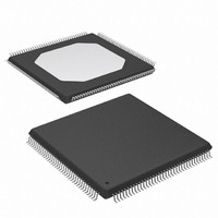
XC3S100E-4TQG144I Xilinx Inc, XC3S100E-4TQG144I Datasheet - Page 49

XC3S100E-4TQG144I
Manufacturer Part Number
XC3S100E-4TQG144I
Description
IC FPGA SPARTAN-3E 100K 144-TQFP
Manufacturer
Xilinx Inc
Series
Spartan™-3Er
Datasheet
1.XC3S100E-4TQG144I.pdf
(193 pages)
Specifications of XC3S100E-4TQG144I
Package / Case
144-TQFP, 144-VQFP
Mounting Type
Surface Mount
Voltage - Supply
1.1 V ~ 3.465 V
Operating Temperature
-40°C ~ 100°C
Number Of I /o
108
Number Of Logic Elements/cells
*
Number Of Gates
*
Lead Free Status / RoHS Status
Lead free / RoHS Compliant
Available stocks
Company
Part Number
Manufacturer
Quantity
Price
Company:
Part Number:
XC3S100E-4TQG144I
Manufacturer:
XILINX/21
Quantity:
163
Company:
Part Number:
XC3S100E-4TQG144I
Manufacturer:
Xilinx Inc
Quantity:
10 000
Part Number:
XC3S100E-4TQG144I
Manufacturer:
XILINX/赛灵思
Quantity:
20 000
Functional Description
In the on-chip synchronization case in
Figure
output clock signals through general routing resources to
the FPGA’s internal registers. Either a Global Clock Buffer
(BUFG) or a BUFGMUX affords access to the global clock
network. As shown in
ated by routing CLK0 (or CLK2X, in
clock net, which in turn drives the CLKFB input.
In the off-chip synchronization case in
Figure
output clock signals exit the FPGA using output buffers
(OBUF) to drive an external clock network plus registers on
the board. As shown in
formed by feeding CLK0 (or CLK2X, in
into the FPGA using an IBUFG, which directly accesses the
global clock network, or an IBUF. Then, the global clock net
is connected directly to the CLKFB input.
Accommodating High Input Frequencies
If the frequency of the CLKIN signal is high such that it
exceeds the maximum permitted, divide it down to an
acceptable value using the CLKIN_DIVIDE_BY_2 attribute.
When this attribute is set to TRUE, the CLKIN frequency is
divided by a factor of two just as it enters the DCM.
42
39b, it is possible to connect any of the DLL’s seven
39d, CLK0 (or CLK2X) plus any of the DLL’s other
BUFG
IBUFG
IBUFG
(a) On-Chip with CLK0 Feedback
(c) Off-Chip with CLK0 Feedback
Figure 39: Input Clock, Output Clock, and Feedback Connections for the DLL
CLKIN
CLKFB
CLKIN
CLKFB
DCM
DCM
Figure
FPGA
Figure
CLK2X180
CLK2X180
FPGA
CLK0
CLK0
CLK180
CLK270
CLK180
CLK270
CLKDV
CLKDV
39a, the feedback loop is cre-
CLK2X
CLK2X
CLK90
CLK90
CLK0
CLK0
39c, the feedback loop is
BUFGMUX
BUFGMUX
Figure 39b
OBUF
OBUF
Figure
Figure 39a
Figure 39c
Net Delay
Clock
Net Delay
to a global
Clock
39d) back
www.xilinx.com
and
and
Coarse Phase Shift Outputs of the DLL Compo-
nent
In addition to CLK0 for zero-phase alignment to the CLKIN
signal, the DLL also provides the CLK90, CLK180, and
CLK270 outputs for 90°, 180°, and 270° phase-shifted sig-
nals, respectively. These signals are described in
Their relative timing is shown in
finer increments than 90°, see
Basic Frequency Synthesis Outputs of the DLL
Component
The DLL component provides basic options for frequency
multiplication and division in addition to the more flexible
synthesis capability of the DFS component, described in a
later section. These operations result in output clock signals
with frequencies that are either a fraction (for division) or a
multiple (for multiplication) of the incoming clock frequency.
The CLK2X output produces an in-phase signal that is twice
the frequency of CLKIN. The CLK2X180 output also dou-
bles the frequency, but is 180° out-of-phase with respect to
CLKIN. The CLKDIV output generates a clock frequency
that is a predetermined fraction of the CLKIN frequency.
The CLKDV_DIVIDE attribute determines the factor used to
divide the CLKIN frequency. The attribute can be set to var-
BUFG
IBUFG
IBUFG
(d) Off-Chip with CLK2X Feedback
(b) On-Chip with CLK2X Feedback
CLKIN
CLKFB
CLKIN
CLKFB
DCM
DCM
FPGA
CLK2X180
CLK2X180
CLK2X
CLK2X
FPGA
CLK180
CLK270
CLK180
CLK270
CLKDV
CLKDV
CLK90
CLK90
CLK2X
CLK2X
CLK0
CLK0
Advance Product Specification
Phase Shifter
DS312-2 (v1.1) March 21, 2005
BUFGMUX
BUFGMUX
OBUF
OBUF
Figure
Net Delay
Clock
Net Delay
40. For control in
DS099-2_09_082104
Clock
(PS).
Table
25.
R


