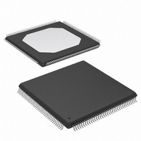
XC3S100E-4TQG144I Xilinx Inc, XC3S100E-4TQG144I Datasheet - Page 74

XC3S100E-4TQG144I
Manufacturer Part Number
XC3S100E-4TQG144I
Description
IC FPGA SPARTAN-3E 100K 144-TQFP
Manufacturer
Xilinx Inc
Series
Spartan™-3Er
Datasheet
1.XC3S100E-4TQG144I.pdf
(193 pages)
Specifications of XC3S100E-4TQG144I
Package / Case
144-TQFP, 144-VQFP
Mounting Type
Surface Mount
Voltage - Supply
1.1 V ~ 3.465 V
Operating Temperature
-40°C ~ 100°C
Number Of I /o
108
Number Of Logic Elements/cells
*
Number Of Gates
*
Lead Free Status / RoHS Status
Lead free / RoHS Compliant
Available stocks
Company
Part Number
Manufacturer
Quantity
Price
Company:
Part Number:
XC3S100E-4TQG144I
Manufacturer:
XILINX/21
Quantity:
163
Company:
Part Number:
XC3S100E-4TQG144I
Manufacturer:
Xilinx Inc
Quantity:
10 000
Part Number:
XC3S100E-4TQG144I
Manufacturer:
XILINX/赛灵思
Quantity:
20 000
Table 47: Serial Peripheral Interface (SPI) Connections (Continued)
Voltage Compatibility
Available SPI Flash PROMs use a single 3.3V supply volt-
age. All of the FPGA’s SPI Flash interface signals are within
DS312-2 (v1.1) March 21, 2005
Advance Product Specification
CSO_B
CCLK
DOUT
INIT_B
DONE
PROG_B
Pin Name
R
FPGA Direction
bidirectional I/O
bidirectional I/O
Open-drain
Open-drain
Output
Output
Output
Input
Chip Select Output. Active Low.
Configuration Clock. Generated
by FPGA internal oscillator.
Frequency controlled by
ConfigRate bitstream generator
option. If CCLK PCB trace is long
or has multiple connections,
terminate this output to maintain
signal integrity.
Serial Data Output.
Initialization Indicator. Active
Low. Goes Low at start of
configuration during Initialization
memory clearing process.
Released at end of memory
clearing, when mode select pins
are sampled. In daisy-chain
applications, this signal requires
an external 4.7 kΩ pull-up resistor
to VCCO_2.
FPGA Configuration Done. Low
during configuration. Goes High
when FPGA successfully
completes configuration. Requires
external 330 Ω pull-up resistor to
2.5V.
Program FPGA. Active Low.
When asserted Low for 300 ns or
longer, forces the FPGA to restart
its configuration process by
clearing configuration memory and
resetting the DONE and INIT_B
pins once PROG_B returns High.
Requires external 4.7 kΩ pull-up
resistor to 2.5V. If driving
externally, use an open-drain or
open-collector driver.
Description
www.xilinx.com
I/O Bank 2. Consequently, the FPGA’s VCCO_2 supply volt-
age must also be 3.3V to match the SPI Flash PROM.
Connects to the SPI Flash
PROM’s chip-select input. If
HSWAP = 1, connect this signal
to a 4.7 kΩ pull-up resistor to
3.3V.
Drives PROM’s clock input.
Actively drives. Not used in
single-FPGA designs. In a
daisy-chain configuration, this
pin connects to DIN input of the
next FPGA in the chain.
Active during configuration. If
SPI Flash PROM requires > 2
ms to awake after powering on,
hold INIT_B Low until PROM is
ready. If CRC error detected
during configuration, FPGA
drives INIT_B Low.
Low indicates that the FPGA is
not yet configured.
Must be High to allow
configuration to start.
During Configuration
Drive CSO_B High after
configuration to disable the
SPI Flash and reclaim the
MOSI, DIN, and CCLK pins.
Optionally, re-use this pin
and MOSI, DIN, and CCLK
to continue communicating
with SPI Flash.
User I/O
User I/O
User I/O
Pulled High via external
pull-up. When High,
indicates that the FPGA
successfully configured.
Drive PROG_B Low and
release to reprogram
FPGA. Hold PROG_B to
force FPGA I/O pins into
Hi-Z, allowing direct
programming access to SPI
Flash PROM pins.
Functional Description
After Configuration
67


