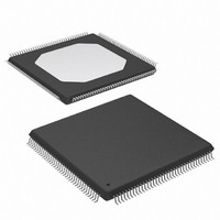
XC3S100E-4TQG144I Xilinx Inc, XC3S100E-4TQG144I Datasheet - Page 47

XC3S100E-4TQG144I
Manufacturer Part Number
XC3S100E-4TQG144I
Description
IC FPGA SPARTAN-3E 100K 144-TQFP
Manufacturer
Xilinx Inc
Series
Spartan™-3Er
Datasheet
1.XC3S100E-4TQG144I.pdf
(193 pages)
Specifications of XC3S100E-4TQG144I
Package / Case
144-TQFP, 144-VQFP
Mounting Type
Surface Mount
Voltage - Supply
1.1 V ~ 3.465 V
Operating Temperature
-40°C ~ 100°C
Number Of I /o
108
Number Of Logic Elements/cells
*
Number Of Gates
*
Lead Free Status / RoHS Status
Lead free / RoHS Compliant
Available stocks
Company
Part Number
Manufacturer
Quantity
Price
Company:
Part Number:
XC3S100E-4TQG144I
Manufacturer:
XILINX/21
Quantity:
163
Company:
Part Number:
XC3S100E-4TQG144I
Manufacturer:
Xilinx Inc
Quantity:
10 000
Part Number:
XC3S100E-4TQG144I
Manufacturer:
XILINX/赛灵思
Quantity:
20 000
Functional Description
Table 25: DLL Signals
Delay-Locked Loop (DLL)
The most basic function of the DLL component is to elimi-
nate clock skew. The main signal path of the DLL consists of
an input stage, followed by a series of discrete delay ele-
ments or taps, which in turn leads to an output stage. This
path together with logic for phase detection and control
forms a system complete with feedback as shown in
Figure
using a counter-based delay line.
The DLL component has two clock inputs, CLKIN and
CLKFB, as well as seven clock outputs, CLK0, CLK90,
CLK180, CLK270, CLK2X, CLK2X180, and CLKDV as
described in
40
CLKIN
CLKFB
CLK0
CLK90
CLK180
CLK270
CLK2X
CLK2X180
CLKDV
Signal
38. In Spartan-3E FPGAs, the DLL is implemented
Table
Direction
25. The clock outputs drive simulta-
Output
Output
Output
Output
Output
Output
Output
Input
Input
CLKFB
CLKIN
RST
Accepts original clock signal.
Accepts either CLK0 or CLK2X as the feedback signal. (Set CLK_FEEDBACK attribute
accordingly).
Generates a clock signal with same frequency and phase as CLKIN.
Generates a clock signal with same frequency as CLKIN, only phase-shifted 90°.
Generates a clock signal with same frequency as CLKIN, only phase-shifted 180°.
Generates a clock signal with same frequency as CLKIN, only phase-shifted 270°.
Generates a clock signal with same phase as CLKIN, only twice the frequency.
Generates a clock signal with twice the frequency of CLKIN, phase-shifted 180° with
respect to CLKIN.
Divides the CLKIN frequency by CLKDV_DIVIDE value to generate lower frequency
clock signal that is phase-aligned to CLKIN.
Figure 38: Simplified Functional Diagram of DLL
Delay
1
Delay
2
Detection
Control
Phase
www.xilinx.com
Delay
n-1
neously. Signals that initialize and report the state of the
DLL are discussed in the Status Logic Component section.
The clock signal supplied to the CLKIN input serves as a
reference waveform. The DLL seeks to align the rising-edge
of feedback signal at the CLKFB input with the rising-edge
of CLKIN input. When eliminating clock skew, the common
approach to using the DLL is as follows: The CLK0 signal is
passed through the clock distribution network to all the reg-
isters it synchronizes. These registers are either internal or
external to the FPGA. After passing through the clock distri-
bution network, the clock signal returns to the DLL via a
feedback line called CLKFB. The control block inside the
DLL measures the phase error between CLKFB and CLKIN.
Delay
n
Description
DS099-2_08_041103
CLK0
CLK90
CLK180
CLK270
CLK2X
CLK2X180
CLKDV
LOCKED
Advance Product Specification
DS312-2 (v1.1) March 21, 2005
R


