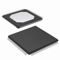
XC3S100E-4TQG144I Xilinx Inc, XC3S100E-4TQG144I Datasheet - Page 73

XC3S100E-4TQG144I
Manufacturer Part Number
XC3S100E-4TQG144I
Description
IC FPGA SPARTAN-3E 100K 144-TQFP
Manufacturer
Xilinx Inc
Series
Spartan™-3Er
Datasheet
1.XC3S100E-4TQG144I.pdf
(193 pages)
Specifications of XC3S100E-4TQG144I
Package / Case
144-TQFP, 144-VQFP
Mounting Type
Surface Mount
Voltage - Supply
1.1 V ~ 3.465 V
Operating Temperature
-40°C ~ 100°C
Number Of I /o
108
Number Of Logic Elements/cells
*
Number Of Gates
*
Lead Free Status / RoHS Status
Lead free / RoHS Compliant
Available stocks
Company
Part Number
Manufacturer
Quantity
Price
Company:
Part Number:
XC3S100E-4TQG144I
Manufacturer:
XILINX/21
Quantity:
163
Company:
Part Number:
XC3S100E-4TQG144I
Manufacturer:
Xilinx Inc
Quantity:
10 000
Part Number:
XC3S100E-4TQG144I
Manufacturer:
XILINX/赛灵思
Quantity:
20 000
Functional Description
Table 46: SPI Flash PROM Connections and Pin Naming (Continued)
The mode select pins, M[2:0], and the variant select pins,
VS[2:0] are sampled when the FPGA’s INIT_B output goes
High and must be at defined logic levels during this time.
After configuration, when the FPGA’s DONE output goes
High, these pins are all available as full-featured user-I/O
pins.
enable pull-up resistors on all user-I/O pins or High to dis-
Table 47: Serial Peripheral Interface (SPI) Connections
66
RESET
(see
RDY/BUSY
(see
P
HSWAP
M[2:0]
VS[2:0]
MOSI
DIN
SPI Flash Pin
Pin Name
P
S
Similarly, the FPGA’s HSWAP pin must be Low to
Figure
Figure
51)
51)
FPGA Direction
Output
Only applicable to Atmel DataFlash. Not
required for FPGA configuration but must be
High during configuration. Optional
connection to FPGA user I/O after
configuration. Do not connect to FPGA’s
PROG_B as this will prevent direct
programming of the DataFlash.
Only applicable to Atmel DataFlash and only
available on certain packages. Not required
for FPGA configuration. Output from
DataFlash PROM. Optional connection to
FPGA user I/O after configuration.
Input
Input
Input
Input
FPGA Connection
User I/O Pull-Up Control. When
Low during configuration, enables
pull-up resistors in all I/O pins to
respective I/O bank V
0: Pull-ups during configuration
1: No pull-ups
Mode Select. Selects the FPGA
configuration mode.
Variant Select. Instructs the
FPGA how to communicate with
the attached SPI Flash PROM.
Serial Data Output.
Serial Data Input.
Description
CCO
www.xilinx.com
input.
able the pull-up resistors. The HSWAP control must remain
at a constant logic level throughout FPGA configuration.
After configuration, when the FPGA’s DONE output goes
High, the HSWAP pin is available as full-featured user-I/O
pin and is powered by the VCCO_0 supply.
In a single-FPGA application, the FPGA’s DOUT pin is not
used but is actively driving during the configuration process.
Drive at valid logic level
throughout configuration.
M2 = 0, M1 = 0, M0 = 1.
Sampled when INIT_B goes
High.
Must be at the logic levels
shown in
when INIT_B goes High.
FPGA sends SPI Flash memory
read commands and starting
address to the PROM’s serial
data input.
FPGA receives serial data from
PROM’s serial data output.
STMicro
During Configuration
N/A
N/A
Table
45. Sampled
NexFlash
N/A
N/A
Advance Product Specification
Technology
DS312-2 (v1.1) March 21, 2005
Storage
Silicon
User I/O
User I/O
User I/O
User I/O
User I/O
N/A
N/A
After Configuration
RDY/BUSY
DataFlash
RESET
Atmel
R


