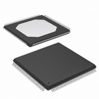
XC3S100E-4TQG144I Xilinx Inc, XC3S100E-4TQG144I Datasheet - Page 140

XC3S100E-4TQG144I
Manufacturer Part Number
XC3S100E-4TQG144I
Description
IC FPGA SPARTAN-3E 100K 144-TQFP
Manufacturer
Xilinx Inc
Series
Spartan™-3Er
Datasheet
1.XC3S100E-4TQG144I.pdf
(193 pages)
Specifications of XC3S100E-4TQG144I
Package / Case
144-TQFP, 144-VQFP
Mounting Type
Surface Mount
Voltage - Supply
1.1 V ~ 3.465 V
Operating Temperature
-40°C ~ 100°C
Number Of I /o
108
Number Of Logic Elements/cells
*
Number Of Gates
*
Lead Free Status / RoHS Status
Lead free / RoHS Compliant
Available stocks
Company
Part Number
Manufacturer
Quantity
Price
Company:
Part Number:
XC3S100E-4TQG144I
Manufacturer:
XILINX/21
Quantity:
163
Company:
Part Number:
XC3S100E-4TQG144I
Manufacturer:
Xilinx Inc
Quantity:
10 000
Part Number:
XC3S100E-4TQG144I
Manufacturer:
XILINX/赛灵思
Quantity:
20 000
- Current page: 140 of 193
- Download datasheet (2Mb)
Footprint Migration Differences
Table 15
ences between the XC3S100E and the XC3S250E FPGAs
that may affect easy migration between devices. There are
four such pins. All other pins not listed in
tionally migrate between Spartan-3E devices available in
the TQ144 package.
Table 15: TQ144 Footprint Migration Differences
The pinout changed slightly between the XC3S100E engi-
neering samples and the production devices, as shown in
Table
M1 and M0 overlap with two global clock inputs feeding the
bottom edge global buffers and DCMs. In the production
devices, the mode pins are swapped with parallel mode
data pins, D1 and D2. This way, these two mode pins do not
interfere with global clock inputs.
DS312-4 (v1.1) March 21, 2005
Advance Product Specification
TQ144 Pin
Legend:
16. In the engineering samples, the mode select pins
P10
P29
P31
P66
DIFFERENCES
summarizes any footprint and functionality differ-
R
This pin can unconditionally migrate from the device on the left to the device on the right. Migration in the other direction may be
possible depending on how the pin is configured for the device on the right.
This pin can unconditionally migrate from the device on the right to the device on the left. Migration in the other direction may be
possible depending on how the pin is configured for the device on the left.
Bank
3
3
3
2
I/O
I/O
VREF(INPUT)
VREF(INPUT)
Table 15
XC3S100E Type
uncondi-
www.xilinx.com
The arrows indicate the direction for easy migration. For
example, a left-facing arrow indicates that the pin on the
XC3S250E unconditionally migrates to the pin on the
XC3S100E. It may be possible to migrate the opposite
direction depending on the I/O configuration. For example,
an I/O pin (Type = I/O) can migrate to an input-only pin
(Type = INPUT) if the I/O pin is configured as an input.
Table 16: XC3S100E Pinout Changes between
Production Devices and Engineering Samples
TQ144 Pin
P58
P59
P60
P62
Migration
4
Production
XC3S100E
D2/GCLK2
D1/GCLK3
Devices
M1
M0
XC3S250E Type
Pinout Descriptions
VREF(I/O)
VREF(I/O)
INPUT
INPUT
Engineering
XC3S100E
M1/GCLK2
M0/GCLK3
Samples
D2
D1
19
Related parts for XC3S100E-4TQG144I
Image
Part Number
Description
Manufacturer
Datasheet
Request
R

Part Number:
Description:
IC SPARTAN-3E FPGA 100K 144-TQFP
Manufacturer:
Xilinx Inc
Datasheet:

Part Number:
Description:
FIELD PROGRAMMER
Manufacturer:
Xilinx Inc
Datasheet:

Part Number:
Description:
FPGA Spartan®-3E Family 100K Gates 2160 Cells 572MHz 90nm (CMOS) Technology 1.2V 100-Pin VTQFP
Manufacturer:
Xilinx Inc
Datasheet:

Part Number:
Description:
FPGA Spartan®-3E Family 100K Gates 2160 Cells 572MHz 90nm (CMOS) Technology 1.2V 144-Pin TQFP
Manufacturer:
Xilinx Inc
Datasheet:

Part Number:
Description:
FPGA Spartan®-3E Family 100K Gates 2160 Cells 657MHz 90nm (CMOS) Technology 1.2V 144-Pin TQFP
Manufacturer:
Xilinx Inc
Datasheet:

Part Number:
Description:
Spartan-3E FPGA Family
Manufacturer:
XILINX [Xilinx, Inc]
Datasheet:

Part Number:
Description:
Spartan-3E FPGA Family: Complete Data Sheet
Manufacturer:
XILINX [Xilinx, Inc]
Datasheet:

Part Number:
Description:
IC FPGA SPARTAN-3E 100K 100-VQFP
Manufacturer:
Xilinx Inc
Datasheet:

Part Number:
Description:
IC FPGA SPARTAN-3E 100K 132CSBGA
Manufacturer:
Xilinx Inc
Datasheet:

Part Number:
Description:
IC FPGA SPARTAN-3E 100K 132CSBGA
Manufacturer:
Xilinx Inc
Datasheet:

Part Number:
Description:
IC FPGA SPARTAN-3E 100K 144-TQFP
Manufacturer:
Xilinx Inc
Datasheet:

Part Number:
Description:
IC FPGA SPARTAN 3E 100VQFP
Manufacturer:
Xilinx Inc
Datasheet:

Part Number:
Description:
IC FPGA SPARTAN 3E 144TQFP
Manufacturer:
Xilinx Inc
Datasheet:

Part Number:
Description:
FPGA Spartan®-3E Family 100K Gates 2160 Cells 572MHz 90nm (CMOS) Technology 1.2V 132-Pin CSBGA
Manufacturer:
Xilinx Inc
Datasheet:

Part Number:
Description:
IC CPLD .8K 36MCELL 44-VQFP
Manufacturer:
Xilinx Inc
Datasheet:


