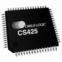
CS42528-DQZ Cirrus Logic Inc, CS42528-DQZ Datasheet - Page 78

CS42528-DQZ
Manufacturer Part Number
CS42528-DQZ
Description
IC CODEC S/PDIF RCVR 64-LQFP
Manufacturer
Cirrus Logic Inc
Type
Audio Codecr
Datasheet
1.CS42528-CQZ.pdf
(91 pages)
Specifications of CS42528-DQZ
Data Interface
Serial
Resolution (bits)
24 b
Number Of Adcs / Dacs
2 / 8
Sigma Delta
Yes
Dynamic Range, Adcs / Dacs (db) Typ
114 / 114
Voltage - Supply, Analog
4.75 V ~ 5.25 V
Voltage - Supply, Digital
3.13 V ~ 5.25 V
Operating Temperature
-40°C ~ 85°C
Mounting Type
Surface Mount
Package / Case
64-LQFP
Audio Codec Type
Stereo
No. Of Adcs
2
No. Of Dacs
8
No. Of Input Channels
2
No. Of Output Channels
8
Adc / Dac Resolution
24bit
Adcs / Dacs Signal To Noise Ratio
114dB
Lead Free Status / RoHS Status
Lead free / RoHS Compliant
For Use With
598-1503 - BOARD EVAL FOR CS42528/CS49300
Lead Free Status / RoHS Status
Lead free / RoHS Compliant, Lead free / RoHS Compliant
Available stocks
Company
Part Number
Manufacturer
Quantity
Price
Company:
Part Number:
CS42528-DQZ
Manufacturer:
Cirrus Logic Inc
Quantity:
10 000
Company:
Part Number:
CS42528-DQZR
Manufacturer:
Cirrus Logic Inc
Quantity:
10 000
CS42528
The external PLL component values listed in
Table 21
have a high corner-frequency jitter-attenuation
curve, take a short time to lock, and offer good output jitter performance. It should be noted that the PLL
component values shown must be used with their associated locking modes as shown in
Table
21. Use
of any other combinations of component values and locking modes may result in unstable PLL behavior.
Configuration 1 may be used for hardware and software backward-compatibility for designs originally
made with the CS42528 Revision C.
Configuration 2 may be used for hardware-only backward-compatibility for designs originally made with
the CS42528 Revision C. Using the Revision D default locking mode of ‘01’ will provide improved wide-
band jitter rejection in Double- and Quad-Speed modes.
Configuration 3 may be used for new designs with the CS42528 Revision D, or for existing designs in
which the hardware and software may be changed to use the specified PLL component values and
LOCKM[1:0] register setting. This configuration provides the best DAC and ADC performance when
clocked from the PLL recovered clock.
The Typical Connection Diagram, Figure 5, shows the recommended configuration of the two capacitors
and one resistor that comprise the PLL filter. It is important to treat the LPFILT pin as a low-level analog
input. It is suggested that the ground end of the PLL filter be returned directly to the AGND pin indepen-
dently of the digital ground plane.
78
DS586F1


