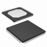
XCCACE-TQG144I Xilinx Inc, XCCACE-TQG144I Datasheet - Page 16

XCCACE-TQG144I
Manufacturer Part Number
XCCACE-TQG144I
Description
IC ACE CONTROLLER CHIP TQ144
Manufacturer
Xilinx Inc
Datasheet
1.XCCACE-TQG144I.pdf
(69 pages)
Specifications of XCCACE-TQG144I
Controller Type
ACE Controller
Voltage - Supply
3 V ~ 3.6 V
Current - Supply
30mA
Operating Temperature
-40°C ~ 85°C
Mounting Type
Surface Mount
Package / Case
144-TQFP, 144-VQFP
Lead Free Status / RoHS Status
Lead free / RoHS Compliant
Interface
-
Other names
122-1511-5
Available stocks
Company
Part Number
Manufacturer
Quantity
Price
Company:
Part Number:
XCCACE-TQG144I
Manufacturer:
XILINX
Quantity:
100
Part Number:
XCCACE-TQG144I
Manufacturer:
XILINX/赛灵思
Quantity:
20 000
Part Number:
XCCACE-TQG144ILEADFREE
Manufacturer:
XILINX/赛灵思
Quantity:
20 000
System ACE CompactFlash Solution
Multiple Register Write Timing
The minimum timing requirements for sequential write
cycles are shown in
Data Buffer Ready Timing
The data buffer ready (MPBRDY) signal indicates whether
the data buffer is ready to accept new data during a write
cycle or whether the data buffer contains valid data to be
read during a read cycle. The data buffer itself is sixteen
words deep, where each word is 16 bits wide.
The data buffer mode transfer direction is identified by the
state of the DATABUFMODE bit in the STATUSREG regis-
ter:
•
16
DATABUFMODE = 0 indicates data buffer read mode
CYCLE
CLK
MPA
MPD
MPCE
MPWE
MPOE
Figure
12. Sequential write cycles are
60ns
Cycle 0
Figure 12: Multiple WORD Writes to ACE Register(s)
80ns
ADDRESS <0>
tSOE
tSCE
tSA
Cycle 1
100ns
DATA <0>
tSWE
tSD
www.xilinx.com
120ns
tH
tH
tH
Cycle 2
tSWE
identical to single write cycles except that the chip enable
(MPCE) and output enable (MPOE) signals do not need to
be de-asserted between write cycles.
•
The data buffer mode depends on the type of command that
was issued to the System ACE CF controller. If an Identi-
fyMemCard or ReadMemCard command was issued, then
the data buffer remains in read mode until the command is
finished executing (i.e., all sector data has been read from
the buffer). If a WriteMemCard command was issued, then
the data buffer remains in write mode until the command is
finished executing (i.e., all sector data has been written to
the buffer).
140ns
ADDRESS <1>
DATABUFMODE = 1 indicates data buffer write mode
tSA
tH
Cycle 3
160ns
DATA <1>
tSWE
tSD
180ns
tH
tH
tH
tH
tH
Cycle 4
tSWE
200ns
DS080 (v2.0) October 1, 2008
DS080_17_020101
Cycle 5
Product Specification
tH
22
R


