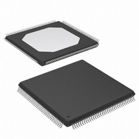
XCCACE-TQG144I Xilinx Inc, XCCACE-TQG144I Datasheet - Page 45

XCCACE-TQG144I
Manufacturer Part Number
XCCACE-TQG144I
Description
IC ACE CONTROLLER CHIP TQ144
Manufacturer
Xilinx Inc
Datasheet
1.XCCACE-TQG144I.pdf
(69 pages)
Specifications of XCCACE-TQG144I
Controller Type
ACE Controller
Voltage - Supply
3 V ~ 3.6 V
Current - Supply
30mA
Operating Temperature
-40°C ~ 85°C
Mounting Type
Surface Mount
Package / Case
144-TQFP, 144-VQFP
Lead Free Status / RoHS Status
Lead free / RoHS Compliant
Interface
-
Other names
122-1511-5
Available stocks
Company
Part Number
Manufacturer
Quantity
Price
Company:
Part Number:
XCCACE-TQG144I
Manufacturer:
XILINX
Quantity:
100
Part Number:
XCCACE-TQG144I
Manufacturer:
XILINX/赛灵思
Quantity:
20 000
Part Number:
XCCACE-TQG144ILEADFREE
Manufacturer:
XILINX/赛灵思
Quantity:
20 000
Read Data Buffer Control Flow Process
The control flow process for reading from the data buffer is
shown in
mented as a 32-byte (16-word) deep FIFO that is aliased
across a range of MPU byte addresses (40h through 7Fh) in
order to facilitate burst transfers across the MPU interface.
Sector data is read from the data buffer by first waiting for
the buffer to become ready (i.e., full of sector data), as
DS080 (v2.0) October 1, 2008
Product Specification
Figure
R
25. The System ACE data buffer is imple-
No
Wait for Buffer Ready
Read Data Buffer
Decrement Data
Buffer is written.
Return success.
Read data word
Count variable*
Figure 25: Read Data Buffer Control Flow Process
Count variable
Initialize Data
from buffer
Data Count
equal to 0?
Yes
www.xilinx.com
*Set Data Count variable equal to
the number of data items in a buffer
(e.g., 16 bytes or 32 words)
Read data bits 7:0 from byte address 40h
Read data bits 15:8 from byte address 41h
(Note that the following conditions must
be valid for a data read to occur from the
CompactFlash data buffer:
1. The data buffer must be ready
2. A single read from byte address 41h
must occur that will cause the entire 16-
bit data register to be overwritten by the
buffer with new data)
shown in
all 32 bytes can be read from the buffer from alternating
even and odd byte addresses. Reading from an odd byte
address while in BYTE mode causes the FIFO to increment
the data word to the next available word in the FIFO. Read-
ing from any data buffer address while in WORD mode will
cause the FIFO to increment.
Figure 26, page
System ACE CompactFlash Solution
DS080_51_051701
46. Once the buffer is ready, then
45


