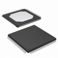
XCCACE-TQG144I Xilinx Inc, XCCACE-TQG144I Datasheet - Page 42

XCCACE-TQG144I
Manufacturer Part Number
XCCACE-TQG144I
Description
IC ACE CONTROLLER CHIP TQ144
Manufacturer
Xilinx Inc
Datasheet
1.XCCACE-TQG144I.pdf
(69 pages)
Specifications of XCCACE-TQG144I
Controller Type
ACE Controller
Voltage - Supply
3 V ~ 3.6 V
Current - Supply
30mA
Operating Temperature
-40°C ~ 85°C
Mounting Type
Surface Mount
Package / Case
144-TQFP, 144-VQFP
Lead Free Status / RoHS Status
Lead free / RoHS Compliant
Interface
-
Other names
122-1511-5
Available stocks
Company
Part Number
Manufacturer
Quantity
Price
Company:
Part Number:
XCCACE-TQG144I
Manufacturer:
XILINX
Quantity:
100
Part Number:
XCCACE-TQG144I
Manufacturer:
XILINX/赛灵思
Quantity:
20 000
Part Number:
XCCACE-TQG144ILEADFREE
Manufacturer:
XILINX/赛灵思
Quantity:
20 000
System ACE CompactFlash Solution
Once the CompactFlash device is ready to receive a new
command, the following information needs to be written to
the MPU interface:
1. The sector address or logical block address (LBA) of
2. The number of sectors to be read should be written to
3. The ReadMemCardData command (03h) should be
42
the first sector to be transferred should be written to the
following MPU address locations:
-
-
-
-
the low byte of the SECCNTCMDREG register (MPU
byte address 14h)
written to the high byte of the SECCNTCMDREG
register (MPU byte address 15h)
LBA[7:0] @ MPU byte address 10h
LBA[15:8] @ MPU byte address 11h
LBA[23:16] @ MPU byte address 12h
LBA[27:24] @ MPU byte address 13h (note that
only four bits are used in the most significant LBA
byte)
www.xilinx.com
4. Reset the CFGJTAG controller by setting the
Immediately after writing the command to the MPU inter-
face, the CFGJTAG controller should be reset before read-
ing the sector data from the data buffer.
The control flow process for reading the sector data from
the data buffer is shown in
After all of the requested sector data has been read, the
CFGJTAG controller should be taken out of reset and the
CompactFlash lock should be released by setting the
LOCKREQ bit (bit 1) and CFGRESET bit (bit 7) of the low
byte of the CONTROLREG register (MPU byte address
18h) to a 0. Note that all requested sector data should be
read from the data buffer in order to avoid a deadlock situa-
tion with the CompactFlash device.
CFGRESET bit (bit 7) of the CONTROLREG register
(MPU address 18h) to a 1.
Figure 25, page
DS080 (v2.0) October 1, 2008
Product Specification
45.
R


