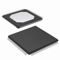
XCCACE-TQG144I Xilinx Inc, XCCACE-TQG144I Datasheet - Page 52

XCCACE-TQG144I
Manufacturer Part Number
XCCACE-TQG144I
Description
IC ACE CONTROLLER CHIP TQ144
Manufacturer
Xilinx Inc
Datasheet
1.XCCACE-TQG144I.pdf
(69 pages)
Specifications of XCCACE-TQG144I
Controller Type
ACE Controller
Voltage - Supply
3 V ~ 3.6 V
Current - Supply
30mA
Operating Temperature
-40°C ~ 85°C
Mounting Type
Surface Mount
Package / Case
144-TQFP, 144-VQFP
Lead Free Status / RoHS Status
Lead free / RoHS Compliant
Interface
-
Other names
122-1511-5
Available stocks
Company
Part Number
Manufacturer
Quantity
Price
Company:
Part Number:
XCCACE-TQG144I
Manufacturer:
XILINX
Quantity:
100
Part Number:
XCCACE-TQG144I
Manufacturer:
XILINX/赛灵思
Quantity:
20 000
Part Number:
XCCACE-TQG144ILEADFREE
Manufacturer:
XILINX/赛灵思
Quantity:
20 000
System ACE CompactFlash Solution
Write Data to CFGJTAG Interface Control Flow
Process
The target devices in the CFGJTAG chain can also be pro-
grammed via the MPU interface as shown in
page
figuration data to the CFGJTAG controller:
1. Arbitrate for the data buffer by requesting a
2. Put the CFGJTAG controller into the reset state by
3. Direct the CFGJTAG controller to wait for CFGSTART=1
4. Directs the CFGJTAG controller to start receiving ACE
5. Release the CFGJTAG controller from the Reset state
6. Initialize the Buffer Count variable.
7. Perform the Write Data Buffer process. All ACE file
52
CompactFlash lock as shown in
Once the lock has been granted, go to
setting CFGRESET=1 (bit 7 of the CONTROLREG
register, MPU byte address 18h).
to begin configuration by setting FORCECFGMODE=1
(bit 3 of the CONTROLREG register, MPU byte address
18h) and CFGMODE=0 (bit 4 of the CONTROLREG
register, MPU byte address 18h).
configuration information from the MPU port when
CFGRESET is released by setting CFGSTART=1 (bit 5
of the CONTROLREG register, MPU byte address 18h)
and CFGSEL=1 (bit 6 of the CONTROLREG register,
MPU byte address 18h).
and cause it to wait for ACE configuration data from the
MPU port by setting CFGRESET=0 (bit 7 of the
CONTROLREG register, MPU byte address 18h).
information should be sent with the exception of the first
512 bytes of the file. Note that an entire buffer’s worth of
53. The following steps should be taken to write con-
Figure 23, page
step
2.
Figure 32,
43.
www.xilinx.com
Notes:
8. Decrement the Buffer Count variable.
9. Check configuration status. If a configuration error
10. Check the Buffer Count variable. If Buffer Count is not 0,
11. Check to see if the configuration process has
12. Set CFGRESET=1 (bit 7 of the CONTROLREG
data should be written to the buffer to ensure that it gets
sent to the CFGJTAG controller.
Note: The first 512 bytes of the ACE file comprise a comment
header and do not contain valid ACE instructions and
therefore should not be written to the CFGJTAG controller via
the MPU port. The configuration engine does this
automatically when processing the ACE file from CF, but it
does not do this for ACE information coming from the MPU
port.Failure to strip off the first 512 bytes will result in
CFGFAILED=1 and CFGINSTRERR=1 in the ERRORREG
register.
exists, stop writing data to the MPU port and return the
error condition. If no error, go to
go back to
step
completed successfully by checking for CFGDONE=1
(bit 7 of the STATUSREG register, MPU byte address
04h). If this is not the case, then other bits of the
STATUSREG and ERRORREG register should indicate
the status of the configuration process. If CFGDONE=1,
then go to
register, MPU byte address 18h) and CFGSTART=0 (bit
5 of the CONTROLREG register, MPU byte address
18h). This puts the configuration engine into the Reset
state and directs it not to start again if CFGRESET is
subsequently released.
11.
step
step
12.
7. If Buffer Count is 0, then go to
DS080 (v2.0) October 1, 2008
step
Product Specification
10.
R


