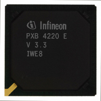
PXB4220E-V33 Infineon Technologies, PXB4220E-V33 Datasheet - Page 30

PXB4220E-V33
Manufacturer Part Number
PXB4220E-V33
Description
IC CHIPSET 8 E1/T1 LINE 256-BGA
Manufacturer
Infineon Technologies
Datasheet
1.PXB4220E-V33.pdf
(290 pages)
Specifications of PXB4220E-V33
Applications
*
Interface
*
Voltage - Supply
*
Package / Case
256-BGA
Mounting Type
Surface Mount
Lead Free Status / RoHS Status
Contains lead / RoHS non-compliant
Other names
PXB4220E-V33
PXB4220E-V33IN
PXB4220E-V33IN
Available stocks
Company
Part Number
Manufacturer
Quantity
Price
Company:
Part Number:
PXB4220E-V33
Manufacturer:
Intel
Quantity:
10
Company:
Part Number:
PXB4220E-V33
Manufacturer:
Infineon Technologies
Quantity:
10 000
- Current page: 30 of 290
- Download datasheet (4Mb)
2.2.6
Table 6
Pin No.
F19, G18,
F20, G19,
G20, H18,
H19, H20,
J17, J18,
J19, J20,
K17, K18,
K19, K20
M18, M17,
N20, N19,
N18, P20,
P19, P18,
R20, R19,
P17, R18,
T19, T18,
U20, V20,
U18, U19,
V19, W19,
Y19, W18,
V17, U16,
W17, V16,
Y17, W16,
V15, U14,
Y16, W15,
V14
M20
L19
M19
Data Sheet
External RAM Interface
Symbol
RMADR[15:0]
RMDAT[32:0]
RMCS
RMOE
RMWR
External RAM Interface
Input (I)
Output (O)
O
Tri
I/O
PUB
O
Tri
O
Tri
O
Tri
30
Function
RAM Address Bus
This bus provides the address of the current
bus cycle. RMADR15 is the MSB.
RAM Data Bus
This bidirectional three-state bus provides
the data path between the IWE8 and the
external memory. RMDAT32 is parity bit,
RMDAT31 is the MSB.
RAM Chip Select
This signal enables read or write accesses
to the external memory
RAM Output Enable
This signal enables the outputs of the
external memory
RAM Write Enable
This output is asserted when a write access
to the external memory
PXB 4219E, PXB 4220E, PXB 4221E
Pin Descriptions
IWE8, V3.4
2003-01-20
Related parts for PXB4220E-V33
Image
Part Number
Description
Manufacturer
Datasheet
Request
R

Part Number:
Description:
IC CHIPSET 8 E1/T1 LINE 256-BGA
Manufacturer:
Infineon Technologies
Datasheet:

Part Number:
Description:
Interworking Element for 8 E1/T1 Lines
Manufacturer:
Infineon Technologies AG
Datasheet:

Part Number:
Description:
members of Infineon ATM Chipset
Manufacturer:
Infineon Technologies AG
Datasheet:

Part Number:
Description:
Manufacturer:
Infineon Technologies AG
Datasheet:

Part Number:
Description:
Manufacturer:
Infineon Technologies AG
Datasheet:

Part Number:
Description:
Manufacturer:
Infineon Technologies AG
Datasheet:

Part Number:
Description:
Manufacturer:
Infineon Technologies AG
Datasheet:

Part Number:
Description:
Manufacturer:
Infineon Technologies AG
Datasheet:

Part Number:
Description:
Manufacturer:
Infineon Technologies AG
Datasheet:

Part Number:
Description:
Manufacturer:
Infineon Technologies AG
Datasheet:

Part Number:
Description:
16-bit microcontroller with 2x2 KByte RAM
Manufacturer:
Infineon Technologies AG
Datasheet:

Part Number:
Description:
NPN silicon RF transistor
Manufacturer:
Infineon Technologies AG
Datasheet:

Part Number:
Description:
NPN silicon RF transistor
Manufacturer:
Infineon Technologies AG
Datasheet:

Part Number:
Description:
NPN silicon RF transistor
Manufacturer:
Infineon Technologies AG
Datasheet:

Part Number:
Description:
NPN silicon RF transistor
Manufacturer:
Infineon Technologies AG
Datasheet:


