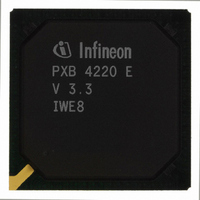
PXB4220E-V33 Infineon Technologies, PXB4220E-V33 Datasheet - Page 51

PXB4220E-V33
Manufacturer Part Number
PXB4220E-V33
Description
IC CHIPSET 8 E1/T1 LINE 256-BGA
Manufacturer
Infineon Technologies
Datasheet
1.PXB4220E-V33.pdf
(290 pages)
Specifications of PXB4220E-V33
Applications
*
Interface
*
Voltage - Supply
*
Package / Case
256-BGA
Mounting Type
Surface Mount
Lead Free Status / RoHS Status
Contains lead / RoHS non-compliant
Other names
PXB4220E-V33
PXB4220E-V33IN
PXB4220E-V33IN
Available stocks
Company
Part Number
Manufacturer
Quantity
Price
Company:
Part Number:
PXB4220E-V33
Manufacturer:
Intel
Quantity:
10
Company:
Part Number:
PXB4220E-V33
Manufacturer:
Infineon Technologies
Quantity:
10 000
- Current page: 51 of 290
- Download datasheet (4Mb)
• For ATM Forum compliance, the “prg_rx_hd” field should be set to 0000 0000.
The deletion of idle, physical layer or unassigned cells can be enabled or disabled per
port by “delete_idle_cells” in the “ATM Receive Reference Slot” of RAM1
(Chapter
4.2.2
Each ATM receive port can be configured in the “channel_mode” field of the “ATM
Receive Reference Slot” in RAM1 to operate in “Inactive”, “Active” or “Standby” mode.
In “Inactive” mode, no data is accepted from the framer receive interface.
In “Active” mode, data is accepted from the framer receive interface, cells are written into
the ATM Receive Buffer and cell addresses are written into the Output Queue.
In “Standby” mode, data is accepted from the framer receive interface but no cells are
written into the ATM Receive Buffer or the Output Queue. This mode can be used to test
the cell delineation.
When activating ATM receive ports, it is important to follow the initialization sequence as
shown in
receive port. During this time the device connected to the Framer Transmit Interface has
to be in normal operation allowing the IWE8 to synchronize itself on the frame pulse.
Table 14
Step
1
2
3
Data Sheet
The “msk_rx_hd” should be set to 1111 1110. This configuration will delete all
unassigned cells.
pcfN.
p_rx_act
0 = inactive
1 = active
1 = active
6.1.1.1).
Table
Setup of ATM Receive Ports
Activation sequence for ATM receive ports
14. Step 2 must be held at least 250 s to internally reset the ATM
ATM Receive Reference Slot.
channel_mode
00 = Inactive
00 = Inactive
01 or 11 = Active
51
PXB 4219E, PXB 4220E, PXB 4221E
Operational Description
Minimum Time
250 s
IWE8, V3.4
2003-01-20
Related parts for PXB4220E-V33
Image
Part Number
Description
Manufacturer
Datasheet
Request
R

Part Number:
Description:
IC CHIPSET 8 E1/T1 LINE 256-BGA
Manufacturer:
Infineon Technologies
Datasheet:

Part Number:
Description:
Interworking Element for 8 E1/T1 Lines
Manufacturer:
Infineon Technologies AG
Datasheet:

Part Number:
Description:
members of Infineon ATM Chipset
Manufacturer:
Infineon Technologies AG
Datasheet:

Part Number:
Description:
Manufacturer:
Infineon Technologies AG
Datasheet:

Part Number:
Description:
Manufacturer:
Infineon Technologies AG
Datasheet:

Part Number:
Description:
Manufacturer:
Infineon Technologies AG
Datasheet:

Part Number:
Description:
Manufacturer:
Infineon Technologies AG
Datasheet:

Part Number:
Description:
Manufacturer:
Infineon Technologies AG
Datasheet:

Part Number:
Description:
Manufacturer:
Infineon Technologies AG
Datasheet:

Part Number:
Description:
Manufacturer:
Infineon Technologies AG
Datasheet:

Part Number:
Description:
16-bit microcontroller with 2x2 KByte RAM
Manufacturer:
Infineon Technologies AG
Datasheet:

Part Number:
Description:
NPN silicon RF transistor
Manufacturer:
Infineon Technologies AG
Datasheet:

Part Number:
Description:
NPN silicon RF transistor
Manufacturer:
Infineon Technologies AG
Datasheet:

Part Number:
Description:
NPN silicon RF transistor
Manufacturer:
Infineon Technologies AG
Datasheet:

Part Number:
Description:
NPN silicon RF transistor
Manufacturer:
Infineon Technologies AG
Datasheet:


