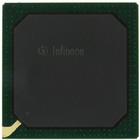
PEB20256E-V21 Infineon Technologies, PEB20256E-V21 Datasheet - Page 72

PEB20256E-V21
Manufacturer Part Number
PEB20256E-V21
Description
IC CONTROLLER INTERFACE 388-BGA
Manufacturer
Infineon Technologies
Datasheet
1.PEB20256E-V21.pdf
(232 pages)
Specifications of PEB20256E-V21
Function
Multichannel Network Interface Controller (MUNICH)
Interface
HDLC, PPP, Serial, TMA
Voltage - Supply
3 V ~ 3.6 V
Current - Supply
200mA
Power (watts)
3W
Operating Temperature
0°C ~ 70°C
Mounting Type
Surface Mount
Package / Case
388-BBGA
Lead Free Status / RoHS Status
Contains lead / RoHS non-compliant
Number Of Circuits
-
Other names
PEB20256E-V21
PEB20256E-V21IN
PEB20256E-V21IN
Available stocks
Company
Part Number
Manufacturer
Quantity
Price
Company:
Part Number:
PEB20256E-V21
Manufacturer:
MAX
Quantity:
63
Company:
Part Number:
PEB20256E-V21
Manufacturer:
Infineon Technologies
Quantity:
10 000
- Current page: 72 of 232
- Download datasheet (3Mb)
Table 4-4
Table 4-5
4.3.7
Data is transmitted beginning with byte zero in increasing order. Vice versa data
received is stored starting with byte zero. The position of byte zero depends on the
selected endian mode.
Each byte itself consists of eight bits starting with bit zero (LSB) up to bit seven (MSB).
Data on the serial line is transmitted starting with the LSB. The first bit received is stored
in bit zero.
4.4
4.4.1
The internal receive buffer provides buffering of frame data and status between the
protocol handler and the receive data management units. Internal buffers are essential
to avoid data loss due to the PCI bus latency, especially in the presence of multiple
devices on the same PCI bus, and to enable a minimized bus utilization through burst
accesses.
The incoming data from the protocol handler is stored in a receive central buffer shared
by all the 256 channels. The buffer is written by the protocol handler every time a
complete DWORD is ready or the last byte of a frame has been received. Each channel
has an individual programmable threshold code, which determines after how many
DWORDs a data transfer into the shared memory is generated. The threshold therefore
defines the maximum burst length for a particular channel in receive direction. A data
transfer is also requested as soon as a frame end has been reached. Programming the
burst length to be greater than 1 DWORD avoids too frequent accesses to the PCI bus,
thereby optimizing use of this resource.
For real time channels with lowest possible latency (example: constant bit rate) a value
of one DWORD can be selected for the burst length.
Data Sheet
BNO
BNO
3
7
Transmission Bit/Byte Ordering
Buffer Management
Internal Receive Buffer
Byte3
-
-
Example for little/big Endian with BNO = 3
Example for little big Endian with BNO = 7
Byte 2
Byte 2
Byte 6
Little Endian
Little Endian
Byte 1
Byte 1
Byte 5
Byte 0
Byte 0
Byte 4
72
Byte 0
Byte 0
Byte 4
Byte 1
Byte 1
Byte 5
Big Endian
Big Endian
Functional Description
Byte 2
Byte 2
Byte 6
PEB 20256 E
PEF 20256 E
Byte3
04.2001
-
-
Related parts for PEB20256E-V21
Image
Part Number
Description
Manufacturer
Datasheet
Request
R

Part Number:
Description:
Manufacturer:
Infineon Technologies AG
Datasheet:

Part Number:
Description:
Manufacturer:
Infineon Technologies AG
Datasheet:

Part Number:
Description:
Manufacturer:
Infineon Technologies AG
Datasheet:

Part Number:
Description:
Manufacturer:
Infineon Technologies AG
Datasheet:

Part Number:
Description:
Manufacturer:
Infineon Technologies AG
Datasheet:

Part Number:
Description:
Manufacturer:
Infineon Technologies AG
Datasheet:

Part Number:
Description:
Manufacturer:
Infineon Technologies AG
Datasheet:

Part Number:
Description:
16-bit microcontroller with 2x2 KByte RAM
Manufacturer:
Infineon Technologies AG
Datasheet:

Part Number:
Description:
NPN silicon RF transistor
Manufacturer:
Infineon Technologies AG
Datasheet:

Part Number:
Description:
NPN silicon RF transistor
Manufacturer:
Infineon Technologies AG
Datasheet:

Part Number:
Description:
NPN silicon RF transistor
Manufacturer:
Infineon Technologies AG
Datasheet:

Part Number:
Description:
NPN silicon RF transistor
Manufacturer:
Infineon Technologies AG
Datasheet:

Part Number:
Description:
Si-MMIC-amplifier in SIEGET 25-technologie
Manufacturer:
Infineon Technologies AG
Datasheet:

Part Number:
Description:
IGBT Power Module
Manufacturer:
Infineon Technologies AG
Datasheet:

Part Number:
Description:
IC for switching-mode power supplies
Manufacturer:
Infineon Technologies AG
Datasheet:


