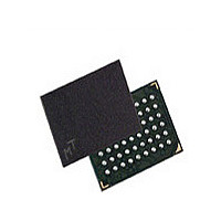
MT48H16M16LFBF-75:H Micron Technology Inc, MT48H16M16LFBF-75:H Datasheet - Page 36

MT48H16M16LFBF-75:H
Manufacturer Part Number
MT48H16M16LFBF-75:H
Description
SDRAM 256M-BIT 1.8V 54-PIN VFBGA
Manufacturer
Micron Technology Inc
Type
Mobile SDRAMr
Datasheet
1.MT48H16M16LFBF-75H.pdf
(86 pages)
Specifications of MT48H16M16LFBF-75:H
Format - Memory
RAM
Memory Type
Mobile SDRAM
Memory Size
256M (16Mx16)
Speed
132MHz
Interface
Parallel
Voltage - Supply
1.7 V ~ 1.95 V
Operating Temperature
0°C ~ 70°C
Package / Case
54-VFBGA
Organization
16Mx16
Density
256Mb
Address Bus
15b
Access Time (max)
8/6ns
Maximum Clock Rate
133MHz
Operating Supply Voltage (typ)
1.8V
Package Type
VFBGA
Operating Temp Range
0C to 70C
Operating Supply Voltage (max)
1.95V
Operating Supply Voltage (min)
1.7V
Supply Current
80mA
Pin Count
54
Mounting
Surface Mount
Operating Temperature Classification
Commercial
Lead Free Status / RoHS Status
Lead free / RoHS Compliant
Other names
Q4707290
Available stocks
Company
Part Number
Manufacturer
Quantity
Price
Company:
Part Number:
MT48H16M16LFBF-75:H
Manufacturer:
MICRON
Quantity:
5 000
Company:
Part Number:
MT48H16M16LFBF-75:H
Manufacturer:
MICRON
Quantity:
5 520
Company:
Part Number:
MT48H16M16LFBF-75:H
Manufacturer:
Micron Technology Inc
Quantity:
10 000
Part Number:
MT48H16M16LFBF-75:H
Manufacturer:
MICRON/美光
Quantity:
20 000
PDF: 09005aef834c13d2
256mb_mobile_sdram_y36n.pdf - Rev. I 11/09 EN
10. For a READ without auto precharge interrupted by a READ (with or without auto pre-
11. For a READ without auto precharge interrupted by a WRITE (with or without auto pre-
12. For a WRITE without auto precharge interrupted by a READ (with or without auto pre-
13. For a WRITE without auto precharge interrupted by a WRITE (with or without auto pre-
14. For a READ with auto precharge interrupted by a READ (with or without auto pre-
15. For a READ with auto precharge interrupted by a WRITE (with or without auto pre-
16. For a WRITE with auto precharge interrupted by a READ (with or without auto pre-
17. For a WRITE with auto precharge interrupted by a WRITE (with or without auto pre-
4. AUTO REFRESH, SELF REFRESH, and LOAD MODE REGISTER commands can only be is-
5. A BURST TERMINATE command cannot be issued to another bank; it applies to the bank
6. All states and sequences not shown are illegal or reserved.
7. READs or WRITEs to bank m listed in the Command/Action column include READs or
8. Concurrent auto precharge: Bank n will initiate the auto precharge command when its
9. The burst in bank n continues as initiated.
Read with auto precharge enabled: Starts with registration of a READ command
with auto precharge enabled and ends when
bank will be in the idle state.
Write with auto precharge enabled: Starts with registration of a WRITE command
with auto precharge enabled and ends when
bank will be in the idle state.
sued when all banks are idle.
represented by the current state only.
WRITEs with auto precharge enabled and READs or WRITEs with auto precharge disabled.
burst has been interrupted by bank m burst.
charge), the READ to bank m will interrupt the READ on bank n, CAS latency (CL) later.
charge), the WRITE to bank m will interrupt the READ on bank n when registered. DQM
should be used one clock prior to the WRITE command to prevent bus contention.
charge), the READ to bank m will interrupt the WRITE on bank n when registered, with
the data-out appearing CL later. The last valid WRITE to bank n will be data-in regis-
tered one clock prior to the READ to bank m.
charge), the WRITE to bank m will interrupt the WRITE on bank n when registered. The
last valid WRITE to bank n will be data-in registered one clock prior to the READ to bank
m.
charge), the READ to bank m will interrupt the READ on bank n, CL later. The PRE-
CHARGE to bank n will begin when the READ to bank m is registered.
charge), the WRITE to bank m will interrupt the READ on bank n when registered. DQM
should be used two clocks prior to the WRITE command to prevent bus contention. The
PRECHARGE to bank n will begin when the WRITE to bank m is registered.
charge), the READ to bank m will interrupt the WRITE on bank n when registered, with
the data-out appearing CL later. The PRECHARGE to bank n will begin after
where
will be data-in registered one clock prior to the READ to bank m.
charge), the WRITE to bank m will interrupt the WRITE on bank n when registered. The
PRECHARGE to bank n will begin after
to bank m is registered. The last valid WRITE to bank n will be data registered one clock
to the WRITE to bank m.
t
WR begins when the READ to bank m is registered. The last valid WRITE bank n
256Mb: 16 Meg x 16, 8 Meg x 32 Mobile SDRAM
36
Micron Technology, Inc. reserves the right to change products or specifications without notice.
t
WR is met, where
t
t
RP has been met. After
RP has been met. After
t
WR begins when the WRITE
©2008 Micron Technology, Inc. All rights reserved.
t
t
RP is met, the
Truth Tables
RP is met, the
t
WR is met,


