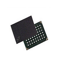
MT48H16M16LFBF-75:H Micron Technology Inc, MT48H16M16LFBF-75:H Datasheet - Page 47

MT48H16M16LFBF-75:H
Manufacturer Part Number
MT48H16M16LFBF-75:H
Description
SDRAM 256M-BIT 1.8V 54-PIN VFBGA
Manufacturer
Micron Technology Inc
Type
Mobile SDRAMr
Datasheet
1.MT48H16M16LFBF-75H.pdf
(86 pages)
Specifications of MT48H16M16LFBF-75:H
Format - Memory
RAM
Memory Type
Mobile SDRAM
Memory Size
256M (16Mx16)
Speed
132MHz
Interface
Parallel
Voltage - Supply
1.7 V ~ 1.95 V
Operating Temperature
0°C ~ 70°C
Package / Case
54-VFBGA
Organization
16Mx16
Density
256Mb
Address Bus
15b
Access Time (max)
8/6ns
Maximum Clock Rate
133MHz
Operating Supply Voltage (typ)
1.8V
Package Type
VFBGA
Operating Temp Range
0C to 70C
Operating Supply Voltage (max)
1.95V
Operating Supply Voltage (min)
1.7V
Supply Current
80mA
Pin Count
54
Mounting
Surface Mount
Operating Temperature Classification
Commercial
Lead Free Status / RoHS Status
Lead free / RoHS Compliant
Other names
Q4707290
Available stocks
Company
Part Number
Manufacturer
Quantity
Price
Company:
Part Number:
MT48H16M16LFBF-75:H
Manufacturer:
MICRON
Quantity:
5 000
Company:
Part Number:
MT48H16M16LFBF-75:H
Manufacturer:
MICRON
Quantity:
5 520
Company:
Part Number:
MT48H16M16LFBF-75:H
Manufacturer:
Micron Technology Inc
Quantity:
10 000
Part Number:
MT48H16M16LFBF-75:H
Manufacturer:
MICRON/美光
Quantity:
20 000
READ Operation
PDF: 09005aef834c13d2
256mb_mobile_sdram_y36n.pdf - Rev. I 11/09 EN
READ bursts are initiated with a READ command, as shown in Figure 9 (page 29). The
starting column and bank addresses are provided with the READ command, and auto
precharge is either enabled or disabled for that burst access. If auto precharge is ena-
bled, the row being accessed is precharged at the completion of the burst. In the
following figures, auto precharge is disabled.
During READ bursts, the valid data-out element from the starting column address is
available following the CAS latency after the READ command. Each subsequent data-
out element will be valid by the next positive clock edge. Figure 18 (page 49) shows
general timing for each possible CAS latency setting.
Upon completion of a burst, assuming no other commands have been initiated, the DQ
signals will go to High-Z. A continuous page burst continues until terminated. At the
end of the page, it wraps to column 0 and continues.
Data from any READ burst can be truncated with a subsequent READ command, and
data from a fixed-length READ burst can be followed immediately by data from a READ
command. In either case, a continuous flow of data can be maintained. The first data
element from the new burst either follows the last element of a completed burst or the
last desired data element of a longer burst that is being truncated. The new READ com-
mand should be issued x cycles before the clock edge at which the last desired data
element is valid, where x = CL - 1. This is shown in Figure 18 (page 49) for CL2 and CL3.
Mobile LPSDR devices use a pipelined architecture and therefore do not require the 2n
rule associated with a prefetch architecture. A READ command can be initiated on any
clock cycle following a READ command. Full-speed random read accesses can be per-
formed to the same bank, or each subsequent READ can be performed to a different bank.
256Mb: 16 Meg x 16, 8 Meg x 32 Mobile SDRAM
47
Micron Technology, Inc. reserves the right to change products or specifications without notice.
©2008 Micron Technology, Inc. All rights reserved.
READ Operation


