DK-DEV-3SL150N Altera, DK-DEV-3SL150N Datasheet - Page 23
DK-DEV-3SL150N
Manufacturer Part Number
DK-DEV-3SL150N
Description
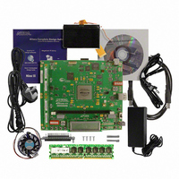
KIT DEVELOPMENT STRATIX III
Manufacturer
Altera
Series
Stratix® IIIr
Type
FPGAr
Datasheets
1.EP3SL150F780C4N.pdf
(16 pages)
2.EP3SL150F780C4N.pdf
(332 pages)
3.DK-DEV-3SL150N.pdf
(34 pages)
Specifications of DK-DEV-3SL150N
Contents
Development Platform, Cables and Software
Silicon Manufacturer
Altera
Core Architecture
FPGA
Core Sub-architecture
Stratix
Silicon Core Number
EP3S
Silicon Family Name
Stratix III
Kit Contents
Development Board, Cable And Accessories
Rohs Compliant
Yes
For Use With/related Products
EP3SL150F152
Lead Free Status / RoHS Status
Lead free / RoHS Compliant
Other names
544-2568
Available stocks
Company
Part Number
Manufacturer
Quantity
Price
Company:

Part Number:
DK-DEV-3SL150N
Manufacturer:
Altera
Quantity:
135


Chapter 1: Stratix III Device Datasheet: DC and Switching Characteristics
Switching Characteristics
Table 1–25. True and Emulated LVDS Specifications for Stratix III Devices
Table 1–26. DPA Lock Time Specifications for Stratix III Devices
© July 2010 Altera Corporation
Non DPA Mode
Sampling Window
Notes to
(1) When J = 3 to 10, the SERDES block is used.
(2) When J = 1 or 2, the SERDES block is bypassed.
(3) Clock Boost Factor (W) is the ratio between the input data rate to the input clock rate.
(4) The minimum and maximum specification depends on the clock source (for example, the PLL and clock pin) and the clock routing resource (global, regional, or
(5) The t
(6) You can estimate the achievable maximum data rate for non-DPA mode by performing link timing closure analysis. Consider the board skew margin, transmitter
(7) This is achieved by using the LVDS and DPA clock network.
(8) If the receiver (with DPA enabled) and the transmitter are using shared PLLs, the minimum data rate is 150 Mbps.
(9) This is only applied to DPA and Soft-CDR modes.
SPI-4
Parallel Rapid
I/O
Standard
local) used. The I/O differential buffer and input register do not have a minimum toggle rate.
delay margin, as well as the receiver sampling margin to determine the maximum data rate supported.
Symbol
Table
xJitter
specification is for the true LVDS I/O standard only.
1–25:
0000000000
1111111111
00001111
10010000
Training
Pattern
Conditions
Table 1–26
—
Transitions
of Training
Repetition
Number of
Pattern
in one
Data
lists the DPA lock time specifications for Stratix III devices.
2
2
4
—
—
repetitions
Number of
Transition
C2
per 256
Data
128
128
(4)
64
300
PLL calibration
PLL calibration
PLL calibration
with DPA PLL
with DPA PLL
with DPA PLL
Condition
without DPA
without DPA
without DPA
calibration
calibration
calibration
—
(Note
C3, I3
—
1), (2),
(5)
(Note
300
3×256 data transitions +
3×256 data transitions +
3×256 data transitions +
(3)
2×96 slow clock cycles
2×96 slow clock cycles
2×96 slow clock cycles
1),
256 data transitions
256 data transitions
256 data transitions
(Part 1 of 2)
(2)
—
(Part 3 of 3)
Min
(6)
(6)
(6)
Stratix III Device Handbook, Volume 2
C4, I4
—
300
Typ
—
—
—
—
—
—
—
C4L, I4L
—
Max
1–23
—
—
—
—
—
—
300
ps
Related parts for DK-DEV-3SL150N
Image
Part Number
Description
Manufacturer
Datasheet
Request
R

Part Number:
Description:
KIT DEV ARRIA II GX FPGA 2AGX125
Manufacturer:
Altera
Datasheet:

Part Number:
Description:
KIT DEV CYCLONE III LS EP3CLS200
Manufacturer:
Altera
Datasheet:

Part Number:
Description:
KIT DEV STRATIX IV FPGA 4SE530
Manufacturer:
Altera
Datasheet:

Part Number:
Description:
KIT DEV FPGA 2AGX260 W/6.375G TX
Manufacturer:
Altera
Datasheet:

Part Number:
Description:
KIT DEV MAX V 5M570Z
Manufacturer:
Altera
Datasheet:

Part Number:
Description:
KIT DEV STRATIX V FPGA 5SGXEA7
Manufacturer:
Altera
Datasheet:

Part Number:
Description:
KIT DEVELOPMENT STRATIX IV
Manufacturer:
Altera
Datasheet:

Part Number:
Description:
KIT DEV ARRIA GX 1AGX60N
Manufacturer:
Altera
Datasheet:
Part Number:
Description:
KIT STARTER CYCLONE IV GX
Manufacturer:
Altera
Datasheet:
Part Number:
Description:
KIT DEVELOPMENT STRATIX IV
Manufacturer:
Altera
Datasheet:

Part Number:
Description:
CPLD, EP610 Family, ECMOS Process, 300 Gates, 16 Macro Cells, 16 Reg., 16 User I/Os, 5V Supply, 35 Speed Grade, 24DIP
Manufacturer:
Altera Corporation
Datasheet:
Part Number:
Description:
CPLD, EP610 Family, ECMOS Process, 300 Gates, 16 Macro Cells, 16 Reg., 16 User I/Os, 5V Supply, 15 Speed Grade, 24DIP
Manufacturer:
Altera Corporation
Datasheet: