DK-DEV-3SL150N Altera, DK-DEV-3SL150N Datasheet - Page 255
DK-DEV-3SL150N
Manufacturer Part Number
DK-DEV-3SL150N
Description
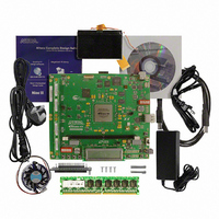
KIT DEVELOPMENT STRATIX III
Manufacturer
Altera
Series
Stratix® IIIr
Type
FPGAr
Datasheets
1.EP3SL150F780C4N.pdf
(16 pages)
2.EP3SL150F780C4N.pdf
(332 pages)
3.DK-DEV-3SL150N.pdf
(34 pages)
Specifications of DK-DEV-3SL150N
Contents
Development Platform, Cables and Software
Silicon Manufacturer
Altera
Core Architecture
FPGA
Core Sub-architecture
Stratix
Silicon Core Number
EP3S
Silicon Family Name
Stratix III
Kit Contents
Development Board, Cable And Accessories
Rohs Compliant
Yes
For Use With/related Products
EP3SL150F152
Lead Free Status / RoHS Status
Lead free / RoHS Compliant
Other names
544-2568
Available stocks
Company
Part Number
Manufacturer
Quantity
Price
Company:

Part Number:
DK-DEV-3SL150N
Manufacturer:
Altera
Quantity:
135


Chapter 1: Stratix III Device Datasheet: DC and Switching Characteristics
I/O Timing
Table 1–119. EP3SE80 Column Pin Delay Adders for Regional Clock
Table 1–120. EP3SE80 Row Pin Delay Adders for Regional Clock
Table 1–121. EP3SE110 Column Pins Input Timing Parameters (Part 1 of 4)
© July 2010 Altera Corporation
RCLK input adder
RCLK PLL input adder
RCLK output adder
RCLK PLL output adder
RCLK input adder
RCLK PLL input adder
RCLK output adder
RCLK PLL output adder
3.3-V LVTTL
3.3-V
LVCMOS
Standard
I/O
Parameter
Parameter
GCLK
GCLK
GCLK
GCLK
Clock
PLL
PLL
t
t
t
t
Table 1–119
must be added to the GCLK values. Use these adder values to determine I/O timing
when the I/O pin is driven using the regional clock. This applies to all I/O standards
supported by Stratix III devices.
Table 1–119
Table 1–120
EP3SE110 I/O Timing Parameters
Table 1–121
EP3SE110 for single-ended I/O standards.
Table 1–121
I/O standards.
t
t
t
t
su
su
su
su
h
h
h
h
Industrial
Industrial
-0.089
-0.069
-1.545
0.014
0.116
0.004
Industrial
0.251
1.895
-1.030
-1.297
-1.030
-1.297
1.172
1.600
1.172
1.600
Fast Model
Fast Model
Fast Model
and
lists the EP3SE80 column pin delay adders when using the regional clock.
lists the EP3SE80 row pin delay adders when using the regional clock.
through
lists the EP3SE110 column pins input timing parameters for single-ended
Commercial
Commercial
Table 1–120
Commercial
-1.367
-0.089
0.187
1.982
0.253
0.003
0.014
0.122
-1.006
-1.267
-1.006
-1.267
1.144
1.565
1.144
1.565
Table 1–124
-1.715 -1.587 -1.976 -3.145 -3.116 -1.541 -3.343 -3.027 -3.123
0.308
2.923
0.551
-0.145 -0.161 -0.197 -0.169 -0.332 -0.151 -0.186 -0.157 -0.333
1.1 V
V
1.1 V
0.018
0.192
0.029
V
list the EP3SE80 regional clock (RCLK) adder values that
-1.454 -1.613 -1.847 -1.786 -2.148 -1.613 -1.847 -1.786 -2.148
-1.831 -2.023 -2.261 -2.187 -2.655 -2.023 -2.261 -2.187 -2.655
-1.454 -1.613 -1.847 -1.786 -2.148 -1.613 -1.847 -1.786 -2.148
-1.831 -2.023 -2.261 -2.187 -2.655 -2.023 -2.261 -2.187 -2.655
C2
1.648
2.262
1.648
2.262
CCL
C2
CCL
1.1 V
V
C2
CCL
=
=
=
list the maximum I/O timing parameters for
0.239
0.865
0.005
0.206
0.042
1.1 V
V
3.16
1.1 V
V
C3
1.838
2.514
1.838
2.514
CCL
C3
1.1 V
CCL
V
C3
CCL
=
=
=
-0.022
0.389
3.601
0.693
0.231
0.056
1.1 V
1.1 V
V
V
C4
2.093
2.793
2.093
2.793
CCL
C4
CCL
1.1 V
V
C4
CCL
=
=
=
-0.059 -0.119
0.039 -0.021 0.047
0.103
0.217
1.1 V
1.1 V
V
V
4.28
0.0
CCL
CCL
2.017
2.689
2.017
2.689
1.1 V
V
CCL
=
=
C4L
C4L
=
C4L
0.052 -0.004 -0.014 -0.008 0.056
0.367
0.176
4.913
0.9 V
0.9 V
V
V
Stratix III Device Handbook, Volume 2
CCL
CCL
2.385
3.180
2.385
3.180
0.9 V
V
=
=
CCL
=
0.198
0.199
3.261
1.1 V
1.1 V
V
V
1.06
I3
CCL
I3
CCL
1.838
2.514
1.838
2.514
1.1 V
V
=
=
I3
CCL
=
0.223
0.061
0.102
4.491
0.135
1.1 V
V
1.1 V
V
CCL
I4
I4
CCL
2.093
2.793
2.093
2.793
1.1 V
V
=
CCL
=
I4
=
0.049
1.1 V
0.099
4.295
0.066
V
0.21
1.1 V
V
1–255
CCL
CCL
2.017
2.689
2.017
2.689
1.1 V
V
=
CCL
=
I4L
I4L
=
-0.025
I4L
0.371
-0.046
0.9 V
V
0.172
4.833
0.9 V
V
CCL
CCL
2.385
3.180
2.385
3.180
0.9 V
V
=
CCL
=
=
Units
Units
ns
ns
ns
ns
ns
ns
ns
ns
Units
ns
ns
ns
ns
ns
ns
ns
ns
Related parts for DK-DEV-3SL150N
Image
Part Number
Description
Manufacturer
Datasheet
Request
R

Part Number:
Description:
KIT DEV ARRIA II GX FPGA 2AGX125
Manufacturer:
Altera
Datasheet:

Part Number:
Description:
KIT DEV CYCLONE III LS EP3CLS200
Manufacturer:
Altera
Datasheet:

Part Number:
Description:
KIT DEV STRATIX IV FPGA 4SE530
Manufacturer:
Altera
Datasheet:

Part Number:
Description:
KIT DEV FPGA 2AGX260 W/6.375G TX
Manufacturer:
Altera
Datasheet:

Part Number:
Description:
KIT DEV MAX V 5M570Z
Manufacturer:
Altera
Datasheet:

Part Number:
Description:
KIT DEV STRATIX V FPGA 5SGXEA7
Manufacturer:
Altera
Datasheet:

Part Number:
Description:
KIT DEVELOPMENT STRATIX IV
Manufacturer:
Altera
Datasheet:

Part Number:
Description:
KIT DEV ARRIA GX 1AGX60N
Manufacturer:
Altera
Datasheet:
Part Number:
Description:
KIT STARTER CYCLONE IV GX
Manufacturer:
Altera
Datasheet:
Part Number:
Description:
KIT DEVELOPMENT STRATIX IV
Manufacturer:
Altera
Datasheet:

Part Number:
Description:
CPLD, EP610 Family, ECMOS Process, 300 Gates, 16 Macro Cells, 16 Reg., 16 User I/Os, 5V Supply, 35 Speed Grade, 24DIP
Manufacturer:
Altera Corporation
Datasheet:
Part Number:
Description:
CPLD, EP610 Family, ECMOS Process, 300 Gates, 16 Macro Cells, 16 Reg., 16 User I/Os, 5V Supply, 15 Speed Grade, 24DIP
Manufacturer:
Altera Corporation
Datasheet: