DK-DEV-3SL150N Altera, DK-DEV-3SL150N Datasheet - Page 5
DK-DEV-3SL150N
Manufacturer Part Number
DK-DEV-3SL150N
Description
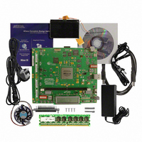
KIT DEVELOPMENT STRATIX III
Manufacturer
Altera
Series
Stratix® IIIr
Type
FPGAr
Datasheets
1.EP3SL150F780C4N.pdf
(16 pages)
2.EP3SL150F780C4N.pdf
(332 pages)
3.DK-DEV-3SL150N.pdf
(34 pages)
Specifications of DK-DEV-3SL150N
Contents
Development Platform, Cables and Software
Silicon Manufacturer
Altera
Core Architecture
FPGA
Core Sub-architecture
Stratix
Silicon Core Number
EP3S
Silicon Family Name
Stratix III
Kit Contents
Development Board, Cable And Accessories
Rohs Compliant
Yes
For Use With/related Products
EP3SL150F152
Lead Free Status / RoHS Status
Lead free / RoHS Compliant
Other names
544-2568
Available stocks
Company
Part Number
Manufacturer
Quantity
Price
Company:

Part Number:
DK-DEV-3SL150N
Manufacturer:
Altera
Quantity:
135


Chapter 1: Stratix III Device Datasheet: DC and Switching Characteristics
Electrical Characteristics
Table 1–6. Bus Hold Parameters for Stratix III Devices (Part 1 of 2)
© July 2010 Altera Corporation
Low sustaining
current
High sustaining
current
Low overdrive
current
Parameter
Symbol
I
I
I
SUSH
SUSL
ODL
DC Characteristics
This section lists the input pin capacitances, on-chip termination tolerance, and
hot- socketing specifications.
Supply Current
Standby current is the current the device draws after the device is configured with no
inputs/outputs toggling and no activity in the device. Because these currents vary
largely with the resources used, use the Excel-based Early Power Estimator (EPE) to
get supply current estimates for your design.
Table 1–4
supply current estimates for the remaining power supplies.
Table 1–4. Supply Current Specifications for V
I/O Pin Leakage Current
Table 1–5
Table 1–5. I/O Pin Leakage Current for Stratix III Devices
Bus Hold Specifications
Table 1–6
I
I
I
I
Notes to
(1) This value is specified for normal device operation. The value may vary during power-up. This applies for all V
(2) The 10-A I/O leakage current limit is applicable when the internal clamping diode is off. A higher current can be
CLKIN
PGM
I
OZ
Symbol
settings (3.3, 3.0, 2.5, 1.8, 1.5, and 1.2 V).
observed when the diode is on.
0V < V
Symbol
Conditions
(maximum)
(minimum)
Table
V
V
IN
IN
lists supply current specifications for V
lists Stratix III I/O pin leakage current specifications.
lists the Stratix III device family bus hold specifications.
IN
> V
< V
Input Pin Leakage Current
Tri-stated I/O Pin Leakage
Current
< V
1–5:
IL
IH
CCIO
V
V
-22.5
Min
22.5
CC_CLKIN
CCPGM
—
Parameter
1.2 V
current specifications
current specifications
Max
120
—
—
-25.0
Min
25.0
—
Parameter
1.5 V
Max
160
—
—
CC_CLKIN
V
V
I
O
= V
= V
-30.0
Conditions
Min
30.0
—
CCIOMAX
CCIOMAX
and V
1.8 V
V
CC_CLKIN
CCIO
(Note
to 0 V
Max
to 0 V
200
—
—
CCPGM
1),
and V
-50.0
Min
50.0
—
(2)
Stratix III Device Handbook, Volume 2
2.5 V
Min
-10
-10
Min
CCPGM
0
0
Max
300
—
—
. Use the EPE to get
Typ
—
—
-70.0
3.0 V/3.3 V
Min
70.0
—
Max
250
250
Max
10
10
Max
500
—
—
Unit
mA
mA
Unit
A
A
Unit
µA
µA
µA
CCIO
1–5
Related parts for DK-DEV-3SL150N
Image
Part Number
Description
Manufacturer
Datasheet
Request
R

Part Number:
Description:
KIT DEV ARRIA II GX FPGA 2AGX125
Manufacturer:
Altera
Datasheet:

Part Number:
Description:
KIT DEV CYCLONE III LS EP3CLS200
Manufacturer:
Altera
Datasheet:

Part Number:
Description:
KIT DEV STRATIX IV FPGA 4SE530
Manufacturer:
Altera
Datasheet:

Part Number:
Description:
KIT DEV FPGA 2AGX260 W/6.375G TX
Manufacturer:
Altera
Datasheet:

Part Number:
Description:
KIT DEV MAX V 5M570Z
Manufacturer:
Altera
Datasheet:

Part Number:
Description:
KIT DEV STRATIX V FPGA 5SGXEA7
Manufacturer:
Altera
Datasheet:

Part Number:
Description:
KIT DEVELOPMENT STRATIX IV
Manufacturer:
Altera
Datasheet:

Part Number:
Description:
KIT DEV ARRIA GX 1AGX60N
Manufacturer:
Altera
Datasheet:
Part Number:
Description:
KIT STARTER CYCLONE IV GX
Manufacturer:
Altera
Datasheet:
Part Number:
Description:
KIT DEVELOPMENT STRATIX IV
Manufacturer:
Altera
Datasheet:

Part Number:
Description:
CPLD, EP610 Family, ECMOS Process, 300 Gates, 16 Macro Cells, 16 Reg., 16 User I/Os, 5V Supply, 35 Speed Grade, 24DIP
Manufacturer:
Altera Corporation
Datasheet:
Part Number:
Description:
CPLD, EP610 Family, ECMOS Process, 300 Gates, 16 Macro Cells, 16 Reg., 16 User I/Os, 5V Supply, 15 Speed Grade, 24DIP
Manufacturer:
Altera Corporation
Datasheet: