DK-DEV-3SL150N Altera, DK-DEV-3SL150N Datasheet - Page 33
DK-DEV-3SL150N
Manufacturer Part Number
DK-DEV-3SL150N
Description
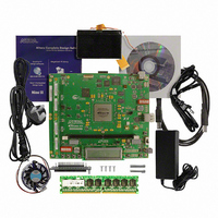
KIT DEVELOPMENT STRATIX III
Manufacturer
Altera
Series
Stratix® IIIr
Type
FPGAr
Datasheets
1.EP3SL150F780C4N.pdf
(16 pages)
2.EP3SL150F780C4N.pdf
(332 pages)
3.DK-DEV-3SL150N.pdf
(34 pages)
Specifications of DK-DEV-3SL150N
Contents
Development Platform, Cables and Software
Silicon Manufacturer
Altera
Core Architecture
FPGA
Core Sub-architecture
Stratix
Silicon Core Number
EP3S
Silicon Family Name
Stratix III
Kit Contents
Development Board, Cable And Accessories
Rohs Compliant
Yes
For Use With/related Products
EP3SL150F152
Lead Free Status / RoHS Status
Lead free / RoHS Compliant
Other names
544-2568
Available stocks
Company
Part Number
Manufacturer
Quantity
Price
Company:

Part Number:
DK-DEV-3SL150N
Manufacturer:
Altera
Quantity:
135


Chapter 1: Stratix III Device Datasheet: DC and Switching Characteristics
I/O Timing
© July 2010 Altera Corporation
5. Compare the results of steps 2 and 4. The increase or decrease in delay must be
The Quartus II software reports the timing with the conditions listed in
using
the output timing of the Quartus II software.
Figure 1–6. Output Delay Timing Report Setup for Single-Ended Outputs and Dedicated Differential
Outputs
Note to
(1) Output pin timing is reported at the output pin of the FPGA device. Additional delays for loading and board trace delay
Figure 1–7
the Quartus II software for differential outputs with single and multiple external
resistors, respectively.
Figure 1–7. Output Delay Timing Report Setup for Differential Outputs with Single External Resistor
Figure 1–8. Output Delay Timing Report Setup for Differential Outputs with Three External Resistor
added to or subtracted from the I/O Standard Output Adder delays to yield the
actual worst-case propagation delay (clock-to-output) of the PCB trace.
must be accounted for with IBIS model simulations.
Figure
Equation 1–1 on page
(Note 1)
and
1–6:
Figure 1–8
Output
Buffer
V
GND
CCIO
Output
show the circuit that is represented by the output timing of
Differential Outputs
Differential Outputs
Non-Dedicated
Non-Dedicated
1–7.
V
MEAS
Figure 1–6
R
S
V
V
V
V
V
GND
MEAS
MEAS
MEAS
MEAS
TT
R
C
shows the circuit that is represented by
T
L
R
R
S
S
R
R
P
P
R
R
D
Stratix III Device Handbook, Volume 2
D
Output
Output
p
n
R
D
Table 1–37
1–33
Related parts for DK-DEV-3SL150N
Image
Part Number
Description
Manufacturer
Datasheet
Request
R

Part Number:
Description:
KIT DEV ARRIA II GX FPGA 2AGX125
Manufacturer:
Altera
Datasheet:

Part Number:
Description:
KIT DEV CYCLONE III LS EP3CLS200
Manufacturer:
Altera
Datasheet:

Part Number:
Description:
KIT DEV STRATIX IV FPGA 4SE530
Manufacturer:
Altera
Datasheet:

Part Number:
Description:
KIT DEV FPGA 2AGX260 W/6.375G TX
Manufacturer:
Altera
Datasheet:

Part Number:
Description:
KIT DEV MAX V 5M570Z
Manufacturer:
Altera
Datasheet:

Part Number:
Description:
KIT DEV STRATIX V FPGA 5SGXEA7
Manufacturer:
Altera
Datasheet:

Part Number:
Description:
KIT DEVELOPMENT STRATIX IV
Manufacturer:
Altera
Datasheet:

Part Number:
Description:
KIT DEV ARRIA GX 1AGX60N
Manufacturer:
Altera
Datasheet:
Part Number:
Description:
KIT STARTER CYCLONE IV GX
Manufacturer:
Altera
Datasheet:
Part Number:
Description:
KIT DEVELOPMENT STRATIX IV
Manufacturer:
Altera
Datasheet:

Part Number:
Description:
CPLD, EP610 Family, ECMOS Process, 300 Gates, 16 Macro Cells, 16 Reg., 16 User I/Os, 5V Supply, 35 Speed Grade, 24DIP
Manufacturer:
Altera Corporation
Datasheet:
Part Number:
Description:
CPLD, EP610 Family, ECMOS Process, 300 Gates, 16 Macro Cells, 16 Reg., 16 User I/Os, 5V Supply, 15 Speed Grade, 24DIP
Manufacturer:
Altera Corporation
Datasheet: