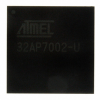
AT32AP7002-CTUT Atmel, AT32AP7002-CTUT Datasheet - Page 178

AT32AP7002-CTUT
Manufacturer Part Number
AT32AP7002-CTUT
Description
IC MCU 32BIT AVR32 196-CBGA
Manufacturer
Atmel
Series
AVR®32 AP7r
Specifications of AT32AP7002-CTUT
Core Processor
AVR
Core Size
32-Bit
Speed
150MHz
Connectivity
EBI/EMI, I²C, MMC, PS2, SPI, SSC, UART/USART, USB
Peripherals
AC'97, DMA, I²C, LCD, POR, PWM, WDT
Number Of I /o
85
Program Memory Type
ROMless
Ram Size
32K x 8
Voltage - Supply (vcc/vdd)
1.65 V ~ 1.95 V
Data Converters
D/A 2x16b
Oscillator Type
Internal
Operating Temperature
-40°C ~ 85°C
Package / Case
196-CBGA
Data Bus Width
32 bit
Data Ram Size
32 KB
Interface Type
I2C, JTAG, PS2, SPI, SSC, UART, USART, USB
Maximum Clock Frequency
150 MHz
Number Of Timers
3
Maximum Operating Temperature
+ 85 C
Mounting Style
SMD/SMT
Minimum Operating Temperature
- 40 C
On-chip Dac
16 bit, 2 Channel
Package
196CTBGA
Device Core
AVR32
Family Name
AT32
Maximum Speed
150 MHz
Operating Supply Voltage
1.8|3.3 V
For Use With
ATAVRONEKIT - KIT AVR/AVR32 DEBUGGER/PROGRMMRATNGW100 - KIT AVR32 NETWORK GATEWAYATSTK1000 - KIT STARTER FOR AVR32AP7000
Lead Free Status / RoHS Status
Lead free / RoHS Compliant
Eeprom Size
-
Program Memory Size
-
Lead Free Status / Rohs Status
Details
Available stocks
Company
Part Number
Manufacturer
Quantity
Price
- Current page: 178 of 896
- Download datasheet (13Mb)
17.10 Programming a Channel
17.10.1
17.10.1.1
32054F–AVR32–09/09
Programming Examples
Single-block Transfer (Row 1)
programmed to zero in the end of block interrupt service routine that services the next-to-last
block transfer. This puts the DMACA into Row 1 state.
For rows 6, 8, and 10 (both CFGx.RELOAD_SR and CFGx.RELOAD_DS cleared) the user must
setup the last block descriptor in memory such that both LLI.CTLx.LLP_S_EN and
LLI.CTLx.LLP_D_EN are zero. If the LLI.LLPx register of the last block descriptor in memory is
non-zero, then the DMA transfer is terminated in Row 5. If the LLI.LLPx register of the last block
descriptor in memory is zero, then the DMA transfer is terminated in Row 1.
For rows 7 and 9, the end-of-block interrupt service routine that services the next-to-last block
transfer should clear the CFGx.RELOAD_SR and CFGx.RELOAD_DS reload bits. The last
block descriptor in memory should be set up so that both the LLI.CTLx.LLP_S_EN and
LLI.CTLx.LLP_D_EN are zero. If the LLI.LLPx register of the last block descriptor in memory is
non-zero, then the DMA transfer is terminated in Row 5. If the LLI.LLPx register of the last block
descriptor in memory is zero, then the DMA transfer is terminated in Row 1.
Note:
Three registers, the LLPx, the CTLx and CFGx, need to be programmed to set up whether single
or multi-block transfers take place, and which type of multi-block transfer is used. The different
transfer types are shown in
The “Update Method” column indicates where the values of SARx, DARx, CTLx, and LLPx are
obtained for the next block transfer when multi-block DMACA transfers are enabled.
Note:
Row 5 in
1. Read the Channel Enable register to choose a free (disabled) channel.
2. Clear any pending interrupts on the channel from the previous DMA transfer by writing to
3. Program the following channel registers:
the Interrupt Clear registers: ClearTfr, ClearBlock, ClearSrcTran, ClearDstTran, ClearErr.
Reading the Interrupt Raw Status and Interrupt Status registers confirms that all inter-
rupts have been cleared.
a. Write the starting source address in the SARx register for channel x.
b. Write the starting destination address in the DARx register for channel x.
c. Program CTLx and CFGx according to Row 1 as shown in
d. Write the control information for the DMA transfer in the CTLx register for channel x.
– i. Set up the transfer type (memory or non-memory peripheral for source and
destination) and flow control device by programming the TT_FC of the CTLx register.
The only allowed transitions between the rows of
row 1 or row 5. As already stated, a transition into row 1 or row 5 is used to terminate the DMA
transfer. All other transitions between rows are not allowed. Software must ensure that illegal tran-
sitions between rows do not occur between blocks of a multi-block transfer. For example, if block N
is in row 10 then the only allowed rows for block N + 1 are rows 10, 5 or 1.
In
CFGx.RELOAD_SR, CTLx.LLP_D_EN, and CFGx.RELOAD_DS are illegal, and causes indeter-
minate or erroneous behavior.
Program the LLPx register with ‘0’.
For example, in the register, you can program the following:
Table 17-1 on page 176
Table 17-1 on page 176
Table 17-1 on page
is also a single block transfer.
, all other combinations of LLPx.LOC = 0, CTLx.LLP_S_EN,
176.
Table 17-1 on page 176
Table 17-1 on page
AT32AP7002
are from any row into
176.
178
Related parts for AT32AP7002-CTUT
Image
Part Number
Description
Manufacturer
Datasheet
Request
R

Part Number:
Description:
DEV KIT FOR AVR/AVR32
Manufacturer:
Atmel
Datasheet:

Part Number:
Description:
INTERVAL AND WIPE/WASH WIPER CONTROL IC WITH DELAY
Manufacturer:
ATMEL Corporation
Datasheet:

Part Number:
Description:
Low-Voltage Voice-Switched IC for Hands-Free Operation
Manufacturer:
ATMEL Corporation
Datasheet:

Part Number:
Description:
MONOLITHIC INTEGRATED FEATUREPHONE CIRCUIT
Manufacturer:
ATMEL Corporation
Datasheet:

Part Number:
Description:
AM-FM Receiver IC U4255BM-M
Manufacturer:
ATMEL Corporation
Datasheet:

Part Number:
Description:
Monolithic Integrated Feature Phone Circuit
Manufacturer:
ATMEL Corporation
Datasheet:

Part Number:
Description:
Multistandard Video-IF and Quasi Parallel Sound Processing
Manufacturer:
ATMEL Corporation
Datasheet:

Part Number:
Description:
High-performance EE PLD
Manufacturer:
ATMEL Corporation
Datasheet:

Part Number:
Description:
8-bit Flash Microcontroller
Manufacturer:
ATMEL Corporation
Datasheet:

Part Number:
Description:
2-Wire Serial EEPROM
Manufacturer:
ATMEL Corporation
Datasheet:


