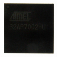
AT32AP7002-CTUT Atmel, AT32AP7002-CTUT Datasheet - Page 737

AT32AP7002-CTUT
Manufacturer Part Number
AT32AP7002-CTUT
Description
IC MCU 32BIT AVR32 196-CBGA
Manufacturer
Atmel
Series
AVR®32 AP7r
Specifications of AT32AP7002-CTUT
Core Processor
AVR
Core Size
32-Bit
Speed
150MHz
Connectivity
EBI/EMI, I²C, MMC, PS2, SPI, SSC, UART/USART, USB
Peripherals
AC'97, DMA, I²C, LCD, POR, PWM, WDT
Number Of I /o
85
Program Memory Type
ROMless
Ram Size
32K x 8
Voltage - Supply (vcc/vdd)
1.65 V ~ 1.95 V
Data Converters
D/A 2x16b
Oscillator Type
Internal
Operating Temperature
-40°C ~ 85°C
Package / Case
196-CBGA
Data Bus Width
32 bit
Data Ram Size
32 KB
Interface Type
I2C, JTAG, PS2, SPI, SSC, UART, USART, USB
Maximum Clock Frequency
150 MHz
Number Of Timers
3
Maximum Operating Temperature
+ 85 C
Mounting Style
SMD/SMT
Minimum Operating Temperature
- 40 C
On-chip Dac
16 bit, 2 Channel
Package
196CTBGA
Device Core
AVR32
Family Name
AT32
Maximum Speed
150 MHz
Operating Supply Voltage
1.8|3.3 V
For Use With
ATAVRONEKIT - KIT AVR/AVR32 DEBUGGER/PROGRMMRATNGW100 - KIT AVR32 NETWORK GATEWAYATSTK1000 - KIT STARTER FOR AVR32AP7000
Lead Free Status / RoHS Status
Lead free / RoHS Compliant
Eeprom Size
-
Program Memory Size
-
Lead Free Status / Rohs Status
Details
Available stocks
Company
Part Number
Manufacturer
Quantity
Price
- Current page: 737 of 896
- Download datasheet (13Mb)
34.4
Table 34-1.
34.5
34.5.1
34.5.2
34.5.3
34.5.4
34.6
32054F–AVR32–09/09
Name
CC
HSYNC
PCLK
VSYNC
DVAL
MOD
PWR
GP[7:0]
LCDD[23:0]
I/O Lines Description
Product Dependencies
Functional Description
I/O Lines
Power Management
Interrupt Sources
Clock Management
I/O Lines Description
Description
Contrast control signal
Line synchronous signal (STN) or Horizontal synchronous signal (TFT)
LCD pixel clock signal (STN/TFT)
Frame synchronous signal (STN) or Vertical synchronization signal (TFT)
STN AC bias signal for the driver or Data enable signal (TFT)
LCD Modulation signal
LCD panel Power enable control signal
LCD General purpose lines
LCD Data Bus output
The pins used for interfacing the LCD Controller may be multiplexed with PIO lines. The pro-
grammer must first program the PIO Controller to assign the pins to their peripheral function. If
I/O lines of the LCD Controller are not used by the application, they can be used for other pur-
poses by the PIO Controller.
The LCDC Core Clock, which is used to generate the PCLK output and the other LCD synchro-
nization signals, is driven by a generic clock output in the Power Manager. Before using the
LCDC, the programmer must ensure that the correct generic clock is enabled in the Power Man-
ager. The generic clock number used for the LCDC is listed in the Power Manager chapter.
The LCD interface has an interrupt line connected to the interrupt controller. In order to handle
interrupts, the interrupt controller must be programmed before configuring the LCD.
When the LCDC is being used in a system with SDRAM, the SDRAM clock frequency must be
greater than the frequency of the LCDC Core Clock.
The LCD Controller consists of two main blocks
and the LCD controller core (LCDC core). The DMA controller reads the display data from an
external memory through a HSB master interface. The LCD controller core formats the display
data. The LCD controller core continuously pumps the pixel data into the LCD module via the
LCD data bus (LCDD[23:0]); this bus is timed by the PCLK, DVAL, HSYNC, and VSYNC signals.
(Figure 34-1 on page
736), the DMA controller
AT32AP7002
Type
Output
Output
Output
Output
Output
Output
Output
Output
Output
737
Related parts for AT32AP7002-CTUT
Image
Part Number
Description
Manufacturer
Datasheet
Request
R

Part Number:
Description:
DEV KIT FOR AVR/AVR32
Manufacturer:
Atmel
Datasheet:

Part Number:
Description:
INTERVAL AND WIPE/WASH WIPER CONTROL IC WITH DELAY
Manufacturer:
ATMEL Corporation
Datasheet:

Part Number:
Description:
Low-Voltage Voice-Switched IC for Hands-Free Operation
Manufacturer:
ATMEL Corporation
Datasheet:

Part Number:
Description:
MONOLITHIC INTEGRATED FEATUREPHONE CIRCUIT
Manufacturer:
ATMEL Corporation
Datasheet:

Part Number:
Description:
AM-FM Receiver IC U4255BM-M
Manufacturer:
ATMEL Corporation
Datasheet:

Part Number:
Description:
Monolithic Integrated Feature Phone Circuit
Manufacturer:
ATMEL Corporation
Datasheet:

Part Number:
Description:
Multistandard Video-IF and Quasi Parallel Sound Processing
Manufacturer:
ATMEL Corporation
Datasheet:

Part Number:
Description:
High-performance EE PLD
Manufacturer:
ATMEL Corporation
Datasheet:

Part Number:
Description:
8-bit Flash Microcontroller
Manufacturer:
ATMEL Corporation
Datasheet:

Part Number:
Description:
2-Wire Serial EEPROM
Manufacturer:
ATMEL Corporation
Datasheet:


