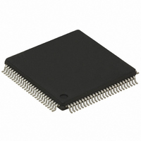
STM32F101V8T6 STMicroelectronics, STM32F101V8T6 Datasheet - Page 16

STM32F101V8T6
Manufacturer Part Number
STM32F101V8T6
Description
MCU ARM 64KB FLASH/TIMER 100LQFP
Manufacturer
STMicroelectronics
Series
STM32r
Datasheet
1.STM32F101T8U6.pdf
(87 pages)
Specifications of STM32F101V8T6
Core Processor
ARM® Cortex-M3™
Core Size
32-Bit
Speed
36MHz
Connectivity
I²C, IrDA, LIN, SPI, UART/USART
Peripherals
DMA, PDR, POR, PVD, PWM, Temp Sensor, WDT
Number Of I /o
80
Program Memory Size
64KB (64K x 8)
Program Memory Type
FLASH
Ram Size
10K x 8
Voltage - Supply (vcc/vdd)
2 V ~ 3.6 V
Data Converters
A/D 16x12b
Oscillator Type
Internal
Operating Temperature
-40°C ~ 85°C
Package / Case
100-LQFP
Processor Series
STM32F101x
Core
ARM Cortex M3
Data Bus Width
32 bit
Data Ram Size
10 KB
Interface Type
I2C, SPI, USART
Maximum Clock Frequency
36 MHz
Number Of Programmable I/os
100
Number Of Timers
3 x 16 bit
Operating Supply Voltage
2 V to 3.6 V
Maximum Operating Temperature
+ 85 C
Mounting Style
SMD/SMT
3rd Party Development Tools
EWARM, EWARM-BL, MDK-ARM, RL-ARM, ULINK2
Minimum Operating Temperature
- 40 C
On-chip Adc
12 bit, 16 Channel
For Use With
497-10030 - STARTER KIT FOR STM32497-8853 - BOARD DEMO STM32 UNIV USB-UUSCIKSDKSTM32-PL - KIT IAR KICKSTART STM32 CORTEXM3497-8512 - KIT STARTER FOR STM32F10XE MCU497-8505 - KIT STARTER FOR STM32F10XE MCU497-8304 - KIT STM32 MOTOR DRIVER BLDC497-6438 - BOARD EVALUTION FOR STM32 512K497-6289 - KIT PERFORMANCE STICK FOR STM32MCBSTM32UME - BOARD EVAL MCBSTM32 + ULINK-MEMCBSTM32U - BOARD EVAL MCBSTM32 + ULINK2497-6053 - KIT STARTER FOR STM32497-6052 - KIT STARTER FOR STM32497-6050 - KIT STARTER FOR STM32497-6049 - KIT EVALUATION LOW COST STM32497-6048 - BOARD EVALUATION FOR STM32497-6047 - KIT DEVELOPMENT FOR STM32497-5046 - KIT TOOL FOR ST7/UPSD/STR7 MCU
Lead Free Status / RoHS Status
Lead free / RoHS Compliant
Eeprom Size
-
Lead Free Status / Rohs Status
Details
Other names
497-6060
Available stocks
Company
Part Number
Manufacturer
Quantity
Price
Company:
Part Number:
STM32F101V8T6
Manufacturer:
DEUTSCH
Quantity:
5 000
Company:
Part Number:
STM32F101V8T6
Manufacturer:
STMicroelectronics
Quantity:
10 000
Part Number:
STM32F101V8T6
Manufacturer:
ST
Quantity:
20 000
Company:
Part Number:
STM32F101V8T6
Manufacturer:
STM
Quantity:
7 908
Company:
Part Number:
STM32F101V8T6TR
Manufacturer:
STMicroelectronics
Quantity:
10 000
Description
2.3.6
2.3.7
2.3.8
2.3.9
2.3.10
16/87
External interrupt/event controller (EXTI)
The external interrupt/event controller consists of 19 edge detector lines used to generate
interrupt/event requests. Each line can be independently configured to select the trigger
event (rising edge, falling edge, both) and can be masked independently. A pending register
maintains the status of the interrupt requests. The EXTI can detect an external line with a
pulse width shorter than the Internal APB2 clock period. Up to 80 GPIOs can be connected
to the 16 external interrupt lines.
Clocks and startup
System clock selection is performed on startup, however the internal RC 8 MHz oscillator is
selected as default CPU clock on reset. An external 4-16 MHz clock can be selected, in
which case it is monitored for failure. If failure is detected, the system automatically switches
back to the internal RC oscillator. A software interrupt is generated if enabled. Similarly, full
interrupt management of the PLL clock entry is available when necessary (for example on
failure of an indirectly used external crystal, resonator or oscillator).
Several prescalers allow the configuration of the AHB frequency, the high-speed APB
(APB2) and the low-speed APB (APB1) domains. The maximum frequency of the AHB and
the APB domains is 36 MHz. See
Boot modes
At startup, boot pins are used to select one of three boot options:
●
●
●
The boot loader is located in System Memory. It is used to reprogram the Flash memory by
using USART1. For further details please refer to AN2606.
Power supply schemes
●
●
●
For more details on how to connect power pins, refer to
Power supply supervisor
The device has an integrated power on reset (POR)/power down reset (PDR) circuitry. It is
always active, and ensures proper operation starting from/down to 2 V. The device remains
in reset mode when V
external reset circuit.
The device features an embedded programmable voltage detector (PVD) that monitors the
V
generated when V
DD
/V
Boot from User Flash
Boot from System Memory
Boot from embedded SRAM
V
Provided externally through V
V
and PLL (minimum voltage to be applied to V
V
V
registers (through power switch) when V
DD
SSA
DDA
BAT
DDA
= 2.0 to 3.6 V: External power supply for I/Os and the internal regulator.
, V
= 1.8 to 3.6 V: Power supply for RTC, external clock 32 kHz oscillator and backup
power supply and compares it to the V
and V
DDA
SSA
= 2.0 to 3.6 V: External analog power supplies for ADC, Reset blocks, RCs
DD
must be connected to V
/V
DD
DDA
is below a specified threshold, V
drops below the V
Doc ID 13586 Rev 14
Figure 2
DD
pins.
for details on the clock tree.
DD
DD
PVD
and V
is not present.
PVD
threshold and/or when V
DDA
SS
threshold. An interrupt can be
is 2.4 V when the ADC is used).
Figure 11: Power supply
, respectively.
POR/PDR
STM32F101x8, STM32F101xB
, without the need for an
DD
/V
DDA
scheme.
is higher


