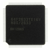
R5F61668RN50FPV Renesas Electronics America, R5F61668RN50FPV Datasheet - Page 1109

R5F61668RN50FPV
Manufacturer Part Number
R5F61668RN50FPV
Description
IC H8SX/1668 MCU FLASH 144LQFP
Manufacturer
Renesas Electronics America
Series
H8® H8SX/1600r
Datasheet
1.R5F61668RN50FPV.pdf
(1506 pages)
Specifications of R5F61668RN50FPV
Core Processor
H8SX
Core Size
16/32-Bit
Speed
50MHz
Connectivity
EBI/EMI, I²C, IrDA, SCI, SmartCard, USB
Peripherals
DMA, LVD, POR, PWM, WDT
Number Of I /o
92
Program Memory Size
1MB (1M x 8)
Program Memory Type
FLASH
Ram Size
56K x 8
Voltage - Supply (vcc/vdd)
3 V ~ 3.6 V
Data Converters
A/D 8x10b; D/A 2x8b
Oscillator Type
External
Operating Temperature
-20°C ~ 75°C
Package / Case
144-LQFP
For Use With
R0K561668S000BE - KIT STARTER FOR H8SX/1668R0K561664S001BE - KIT STARTER FOR H8SX/1651HS0005KCU11H - EMULATOR E10A-USB H8S(X),SH2(A)
Lead Free Status / RoHS Status
Lead free / RoHS Compliant
Eeprom Size
-
Available stocks
Company
Part Number
Manufacturer
Quantity
Price
Company:
Part Number:
R5F61668RN50FPV
Manufacturer:
Renesas Electronics America
Quantity:
10 000
- Current page: 1109 of 1506
- Download datasheet (9Mb)
22.3.3
ADCSR_1 controls A/D conversion operations.
Bit
7
6
5
Bit
Bit Name
Initial Value
R/W
Note: * Only 0 can be written to this bit, to clear the flag.
Bit Name
ADF
ADIE
ADST
A/D Control/Status Register for Unit 1 (ADCSR_1)
R/(W)*
ADF
7
0
Initial
Value
0
0
0
ADIE
R/W
6
0
R/W
R/(W)* A/D End Flag
R/W
R/W
ADST
R/W
5
0
Description
A status flag that indicates the end of A/D conversion.
[Setting conditions]
•
•
[Clearing conditions]
•
•
A/D Interrupt Enable
Setting this bit to 1 enables ADI interrupts by ADF.
A/D Start
Clearing this bit to 0 stops A/D conversion, and the A/D
converter enters wait state.
Setting this bit to 1 starts A/D conversion. In single mode,
this bit is cleared to 0 automatically when A/D conversion
on the specified channel ends. In scan mode, A/D
conversion continues sequentially on the specified
channels until this bit is cleared to 0 by software, a reset,
or hardware standby mode.
Note: Do not write to ADST when activation is by an
Completion of A/D conversion in single mode
Completion of A/D conversion on all specified
channels in scan mode
Writing of 0 after reading ADF = 1
(When the CPU is used to clear this flag by writing 0
while the corresponding interrupt is enabled, be sure
to read the flag after writing 0 to it.)
Reading from ADDR after activation of the DMAC or
DTC by an ADI interrupt
EXCKS
R/W
external trigger. For details, see section 22.7.3,
Notes on A/D activation by an External Trigger.
4
0
CH3
R/W
3
0
Rev. 2.00 Sep. 24, 2008 Page 1075 of 1468
CH2
R/W
2
0
Section 22 A/D Converter
CH1
R/W
1
0
REJ09B0412-0200
CH0
R/W
0
0
Related parts for R5F61668RN50FPV
Image
Part Number
Description
Manufacturer
Datasheet
Request
R

Part Number:
Description:
KIT STARTER FOR M16C/29
Manufacturer:
Renesas Electronics America
Datasheet:

Part Number:
Description:
KIT STARTER FOR R8C/2D
Manufacturer:
Renesas Electronics America
Datasheet:

Part Number:
Description:
R0K33062P STARTER KIT
Manufacturer:
Renesas Electronics America
Datasheet:

Part Number:
Description:
KIT STARTER FOR R8C/23 E8A
Manufacturer:
Renesas Electronics America
Datasheet:

Part Number:
Description:
KIT STARTER FOR R8C/25
Manufacturer:
Renesas Electronics America
Datasheet:

Part Number:
Description:
KIT STARTER H8S2456 SHARPE DSPLY
Manufacturer:
Renesas Electronics America
Datasheet:

Part Number:
Description:
KIT STARTER FOR R8C38C
Manufacturer:
Renesas Electronics America
Datasheet:

Part Number:
Description:
KIT STARTER FOR R8C35C
Manufacturer:
Renesas Electronics America
Datasheet:

Part Number:
Description:
KIT STARTER FOR R8CL3AC+LCD APPS
Manufacturer:
Renesas Electronics America
Datasheet:

Part Number:
Description:
KIT STARTER FOR RX610
Manufacturer:
Renesas Electronics America
Datasheet:

Part Number:
Description:
KIT STARTER FOR R32C/118
Manufacturer:
Renesas Electronics America
Datasheet:

Part Number:
Description:
KIT DEV RSK-R8C/26-29
Manufacturer:
Renesas Electronics America
Datasheet:

Part Number:
Description:
KIT STARTER FOR SH7124
Manufacturer:
Renesas Electronics America
Datasheet:

Part Number:
Description:
KIT STARTER FOR H8SX/1622
Manufacturer:
Renesas Electronics America
Datasheet:

Part Number:
Description:
KIT DEV FOR SH7203
Manufacturer:
Renesas Electronics America
Datasheet:


