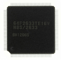
R5F61668RN50FPV Renesas Electronics America, R5F61668RN50FPV Datasheet - Page 1237

R5F61668RN50FPV
Manufacturer Part Number
R5F61668RN50FPV
Description
IC H8SX/1668 MCU FLASH 144LQFP
Manufacturer
Renesas Electronics America
Series
H8® H8SX/1600r
Datasheet
1.R5F61668RN50FPV.pdf
(1506 pages)
Specifications of R5F61668RN50FPV
Core Processor
H8SX
Core Size
16/32-Bit
Speed
50MHz
Connectivity
EBI/EMI, I²C, IrDA, SCI, SmartCard, USB
Peripherals
DMA, LVD, POR, PWM, WDT
Number Of I /o
92
Program Memory Size
1MB (1M x 8)
Program Memory Type
FLASH
Ram Size
56K x 8
Voltage - Supply (vcc/vdd)
3 V ~ 3.6 V
Data Converters
A/D 8x10b; D/A 2x8b
Oscillator Type
External
Operating Temperature
-20°C ~ 75°C
Package / Case
144-LQFP
For Use With
R0K561668S000BE - KIT STARTER FOR H8SX/1668R0K561664S001BE - KIT STARTER FOR H8SX/1651HS0005KCU11H - EMULATOR E10A-USB H8S(X),SH2(A)
Lead Free Status / RoHS Status
Lead free / RoHS Compliant
Eeprom Size
-
Available stocks
Company
Part Number
Manufacturer
Quantity
Price
Company:
Part Number:
R5F61668RN50FPV
Manufacturer:
Renesas Electronics America
Quantity:
10 000
- Current page: 1237 of 1506
- Download datasheet (9Mb)
25.14
1. The initial state of the product at its shipment is in the erased state. For the product whose
2. For the PROM programmer suitable for programmer mode in this LSI and its program version,
3. If the socket, socket adapter, or product index of the PROM programmer do not match the
4. Use a PROM programmer that supports the device with 1-Mbyte on-chip flash memory and
5. Do not turn off the Vcc power supply nor remove the chip from the PROM programmer during
6. The flash memory is not accessible until FKEY is cleared after programming/erasure starts. If
7. At powering on or off the Vcc power supply, fix the RES pin to low and set the flash memory
8. In on-board programming mode or programmer mode, programming of the 128-byte
9. When the chip is to be reprogrammed with the programmer after execution of programming or
10. To program the flash memory, the program data and program must be allocated to addresses
11. The programming program that includes the initialization routine and the erasing program that
revision of erasing is undefined, we recommend to execute automatic erasure for checking the
initial state (erased state) and compensating.
refer to the instruction manual of the socket adapter.
specifications, too much current flows and the product may be damaged.
3.3-V programming voltage. Use only the specified socket adapter.
programming/erasure in which a high voltage is applied to the flash memory. Doing so may
damage the flash memory permanently. If a reset is input, the reset must be released after the
reset input period of at least 100ms.
the operating mode is changed and this LSI is restarted by a reset immediately after
programming/erasure has finished, secure the reset input period (period of RES = 0) of at least
100µs. Transition to the reset state during programming/erasure is inhibited. If a reset is input
accidentally, the reset must be released after the reset input period of at least 100µs.
to hardware protection state. This power on/off timing must also be satisfied at a power-off and
power-on caused by a power failure and other factors.
programming-unit block must be performed only once. Perform programming in the state
where the programming-unit block is fully erased.
erasure in on-board programming mode, it is recommended that automatic programming is
performed after execution of automatic erasure.
which are higher than those of the external interrupt vector table and H'FF must be written to
all the system reserved areas in the exception handling vector table.
includes the initialization routine are each 4 Kbytes or less. Accordingly, when the CPU clock
frequency is 35 MHz, the download for each program takes approximately 60 µs at the
maximum.
Usage Notes
Rev. 2.00 Sep. 24, 2008 Page 1203 of 1468
Section 25 Flash Memory
REJ09B0412-0200
Related parts for R5F61668RN50FPV
Image
Part Number
Description
Manufacturer
Datasheet
Request
R

Part Number:
Description:
KIT STARTER FOR M16C/29
Manufacturer:
Renesas Electronics America
Datasheet:

Part Number:
Description:
KIT STARTER FOR R8C/2D
Manufacturer:
Renesas Electronics America
Datasheet:

Part Number:
Description:
R0K33062P STARTER KIT
Manufacturer:
Renesas Electronics America
Datasheet:

Part Number:
Description:
KIT STARTER FOR R8C/23 E8A
Manufacturer:
Renesas Electronics America
Datasheet:

Part Number:
Description:
KIT STARTER FOR R8C/25
Manufacturer:
Renesas Electronics America
Datasheet:

Part Number:
Description:
KIT STARTER H8S2456 SHARPE DSPLY
Manufacturer:
Renesas Electronics America
Datasheet:

Part Number:
Description:
KIT STARTER FOR R8C38C
Manufacturer:
Renesas Electronics America
Datasheet:

Part Number:
Description:
KIT STARTER FOR R8C35C
Manufacturer:
Renesas Electronics America
Datasheet:

Part Number:
Description:
KIT STARTER FOR R8CL3AC+LCD APPS
Manufacturer:
Renesas Electronics America
Datasheet:

Part Number:
Description:
KIT STARTER FOR RX610
Manufacturer:
Renesas Electronics America
Datasheet:

Part Number:
Description:
KIT STARTER FOR R32C/118
Manufacturer:
Renesas Electronics America
Datasheet:

Part Number:
Description:
KIT DEV RSK-R8C/26-29
Manufacturer:
Renesas Electronics America
Datasheet:

Part Number:
Description:
KIT STARTER FOR SH7124
Manufacturer:
Renesas Electronics America
Datasheet:

Part Number:
Description:
KIT STARTER FOR H8SX/1622
Manufacturer:
Renesas Electronics America
Datasheet:

Part Number:
Description:
KIT DEV FOR SH7203
Manufacturer:
Renesas Electronics America
Datasheet:


