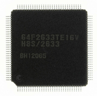
R5F61668RN50FPV Renesas Electronics America, R5F61668RN50FPV Datasheet - Page 267

R5F61668RN50FPV
Manufacturer Part Number
R5F61668RN50FPV
Description
IC H8SX/1668 MCU FLASH 144LQFP
Manufacturer
Renesas Electronics America
Series
H8® H8SX/1600r
Datasheet
1.R5F61668RN50FPV.pdf
(1506 pages)
Specifications of R5F61668RN50FPV
Core Processor
H8SX
Core Size
16/32-Bit
Speed
50MHz
Connectivity
EBI/EMI, I²C, IrDA, SCI, SmartCard, USB
Peripherals
DMA, LVD, POR, PWM, WDT
Number Of I /o
92
Program Memory Size
1MB (1M x 8)
Program Memory Type
FLASH
Ram Size
56K x 8
Voltage - Supply (vcc/vdd)
3 V ~ 3.6 V
Data Converters
A/D 8x10b; D/A 2x8b
Oscillator Type
External
Operating Temperature
-20°C ~ 75°C
Package / Case
144-LQFP
For Use With
R0K561668S000BE - KIT STARTER FOR H8SX/1668R0K561664S001BE - KIT STARTER FOR H8SX/1651HS0005KCU11H - EMULATOR E10A-USB H8S(X),SH2(A)
Lead Free Status / RoHS Status
Lead free / RoHS Compliant
Eeprom Size
-
Available stocks
Company
Part Number
Manufacturer
Quantity
Price
Company:
Part Number:
R5F61668RN50FPV
Manufacturer:
Renesas Electronics America
Quantity:
10 000
- Current page: 267 of 1506
- Download datasheet (9Mb)
(4)
(a)
The number of access cycles in the basic bus interface can be specified as two or three cycles by
the ASTCR. An area specified as 2-state access is specified as 2-state access space; an area
specified as 3-state access is specified as 3-state access space.
For the 2-state access space, a wait cycle insertion is disabled. For the 3-state access space, a
program wait (0 to 7 cycles) specified by WTCRA and WTCRB or an external wait by WAIT can
be inserted.
Assertion period of the chip select signal can be extended by CSACR.
(b) Byte Control SRAM Interface
The number of access cycles in the byte control SRAM interface is the same as that in the basic
bus interface.
(c)
The number of access cycles at full access in the burst ROM interface is the same as that in the
basic bus interface. The number of access cycles in the burst access can be specified as one to
eight cycles by the BSTS bit in BROMCR.
Number of Access Cycles
Basic Bus Interface
Burst ROM Interface
Number of access cycles in the basic bus interface
= number of basic cycles (2, 3) + number of program wait cycles (0 to 7)
Number of access cycles in byte control SRAM interface
= number of basic cycles (2, 3) + number of program wait cycles (0 to 7)
Number of access cycles in the burst ROM interface
= number of basic cycles (2, 3) + number of program wait cycles (0 to 7)
+ number of CS extension cycles (0, 1, 2)
[+ number of external wait cycles by the WAIT pin]
+ number of CS extension cycles (0, 1, 2)
[+ number of external wait cycles by the WAIT pin]
+ number of CS extension cycles (0, 1)
[+number of external wait cycles by the WAIT pin]
+ number of burst access cycles (1 to 8) × number of burst accesses (0 to 63)
Rev. 2.00 Sep. 24, 2008 Page 233 of 1468
Section 9 Bus Controller (BSC)
REJ09B0412-0200
Related parts for R5F61668RN50FPV
Image
Part Number
Description
Manufacturer
Datasheet
Request
R

Part Number:
Description:
KIT STARTER FOR M16C/29
Manufacturer:
Renesas Electronics America
Datasheet:

Part Number:
Description:
KIT STARTER FOR R8C/2D
Manufacturer:
Renesas Electronics America
Datasheet:

Part Number:
Description:
R0K33062P STARTER KIT
Manufacturer:
Renesas Electronics America
Datasheet:

Part Number:
Description:
KIT STARTER FOR R8C/23 E8A
Manufacturer:
Renesas Electronics America
Datasheet:

Part Number:
Description:
KIT STARTER FOR R8C/25
Manufacturer:
Renesas Electronics America
Datasheet:

Part Number:
Description:
KIT STARTER H8S2456 SHARPE DSPLY
Manufacturer:
Renesas Electronics America
Datasheet:

Part Number:
Description:
KIT STARTER FOR R8C38C
Manufacturer:
Renesas Electronics America
Datasheet:

Part Number:
Description:
KIT STARTER FOR R8C35C
Manufacturer:
Renesas Electronics America
Datasheet:

Part Number:
Description:
KIT STARTER FOR R8CL3AC+LCD APPS
Manufacturer:
Renesas Electronics America
Datasheet:

Part Number:
Description:
KIT STARTER FOR RX610
Manufacturer:
Renesas Electronics America
Datasheet:

Part Number:
Description:
KIT STARTER FOR R32C/118
Manufacturer:
Renesas Electronics America
Datasheet:

Part Number:
Description:
KIT DEV RSK-R8C/26-29
Manufacturer:
Renesas Electronics America
Datasheet:

Part Number:
Description:
KIT STARTER FOR SH7124
Manufacturer:
Renesas Electronics America
Datasheet:

Part Number:
Description:
KIT STARTER FOR H8SX/1622
Manufacturer:
Renesas Electronics America
Datasheet:

Part Number:
Description:
KIT DEV FOR SH7203
Manufacturer:
Renesas Electronics America
Datasheet:


