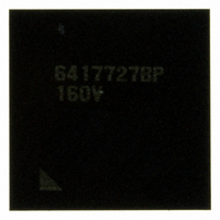
HD6417727BP160CV Renesas Electronics America, HD6417727BP160CV Datasheet - Page 609

HD6417727BP160CV
Manufacturer Part Number
HD6417727BP160CV
Description
IC SH MPU ROMLESS 240BGA
Manufacturer
Renesas Electronics America
Series
SuperH® SH7700r
Datasheet
1.HD6417727BP100CV.pdf
(1098 pages)
Specifications of HD6417727BP160CV
Core Processor
SH-3 DSP
Core Size
32-Bit
Speed
160MHz
Connectivity
FIFO, SCI, SIO, SmartCard, USB
Peripherals
DMA, LCD, POR, WDT
Number Of I /o
104
Program Memory Type
ROMless
Ram Size
32K x 8
Voltage - Supply (vcc/vdd)
1.7 V ~ 2.05 V
Data Converters
A/D 6x10b; D/A 2x8b
Oscillator Type
Internal
Operating Temperature
-20°C ~ 75°C
Package / Case
240-BGA
Package
240CSP
Family Name
SuperH
Maximum Speed
160 MHz
Operating Supply Voltage
1.8|3.3 V
Data Bus Width
32 Bit
Number Of Programmable I/os
104
Interface Type
SCI/USB
On-chip Adc
6-chx10-bit
On-chip Dac
2-chx8-bit
Number Of Timers
4
Lead Free Status / RoHS Status
Lead free / RoHS Compliant
Eeprom Size
-
Program Memory Size
-
Available stocks
Company
Part Number
Manufacturer
Quantity
Price
Company:
Part Number:
HD6417727BP160CV
Manufacturer:
LITEON
Quantity:
46 000
Company:
Part Number:
HD6417727BP160CV
Manufacturer:
Renesas Electronics America
Quantity:
10 000
- Current page: 609 of 1098
- Download datasheet (7Mb)
18.3.4
Table 18.3 shows the bit map of the registers that the smart card interface uses. Bits shown as 1 or
0 must be set to the indicated value. The settings for the other bits are described below.
Table 18.3 Register Settings for the Smart Card Interface
Register
SCSMR
SCBRR
SCSCR
SCTDR
SCSSR
SCRDR
SCSCMR
Note: Dashes indicate unused bits.
1. Setting the serial mode register (SCSMR): The C/A bit selects the set timing of the TEND flag,
2. Setting the bit rate register (SCBRR): Set the bit rate. See section 18.3.5, Clock, to see how to
3. Setting the serial control register (SCSCR): The TIE, RIE, TE and RE bits function as they do
4. Setting the smart card mode register (SCSCMR): The SDIR and SINV bits are both set to 0 for
and selects the clock output state with the combination of bits CKE1 and CKE0 in the serial
control register (SCSCR). Set the O/E bit to 0 when the IC card uses the direct convention or
to 1 when it uses the inverse convention. Select the on-chip baud rate generator clock source
with the CKS1 and CKS0 bits (see section 18.3.5, Clock).
calculate the set value.
for the ordinary SCI0. See section 17, Serial Communication Interface (SCI), for more
information. The CKE0 bit specifies the clock output. When no clock is output, set 0; when a
clock is output, set 1.
IC cards that use the direct convention and both to 1 when the inverse convention is used. The
SMIF bit is set to 1 for the smart card interface.
Figure 18.4 shows sample waveforms for register settings of the two types of IC cards (direct
convention and inverse convention) and their start characters.
In the direct convention type, the logical 1 level is state Z, the logical 0 level is state A, and
communication is LSB first. The start character data is H'3B. The parity bit is even (from the
smart card standards), and thus 1.
Register Settings
H'FFFFFE82
H'FFFFFE84
H'FFFFFE86
H'FFFFFE88
H'FFFFFE8A
Address
H'FFFFFE80
H'FFFFFE8C
Bit 7
C/A
BRR7
TIE
TDR7
TDRE
RDR7
—
Bit 6
0
BRR6
RIE
TDR6
RDRF
RDR6
—
Bit 5
1
BRR5
TE
TDR5
ORER
RDR5
—
Bit 4
O/E
BRR4
RE
TDR4
FER/
ERS
RDR4
—
Rev.6.00 Mar. 27, 2009 Page 551 of 1036
Bit 3
1
BRR3
0
TDR3
PER
RDR3
SDIR
Section 18 Smart Card Interface
Bit 2
BRR2
0
TDR2
TEND
RDR2
0
SINV
REJ09B0254-0600
Bit 1
CKS1
BRR1
CKE1
TDR1
0
RDR1
—
BRR0
CKE0
Bit 0
CKS0
TDR0
0
RDR0
SMIF
Related parts for HD6417727BP160CV
Image
Part Number
Description
Manufacturer
Datasheet
Request
R

Part Number:
Description:
KIT STARTER FOR M16C/29
Manufacturer:
Renesas Electronics America
Datasheet:

Part Number:
Description:
KIT STARTER FOR R8C/2D
Manufacturer:
Renesas Electronics America
Datasheet:

Part Number:
Description:
R0K33062P STARTER KIT
Manufacturer:
Renesas Electronics America
Datasheet:

Part Number:
Description:
KIT STARTER FOR R8C/23 E8A
Manufacturer:
Renesas Electronics America
Datasheet:

Part Number:
Description:
KIT STARTER FOR R8C/25
Manufacturer:
Renesas Electronics America
Datasheet:

Part Number:
Description:
KIT STARTER H8S2456 SHARPE DSPLY
Manufacturer:
Renesas Electronics America
Datasheet:

Part Number:
Description:
KIT STARTER FOR R8C38C
Manufacturer:
Renesas Electronics America
Datasheet:

Part Number:
Description:
KIT STARTER FOR R8C35C
Manufacturer:
Renesas Electronics America
Datasheet:

Part Number:
Description:
KIT STARTER FOR R8CL3AC+LCD APPS
Manufacturer:
Renesas Electronics America
Datasheet:

Part Number:
Description:
KIT STARTER FOR RX610
Manufacturer:
Renesas Electronics America
Datasheet:

Part Number:
Description:
KIT STARTER FOR R32C/118
Manufacturer:
Renesas Electronics America
Datasheet:

Part Number:
Description:
KIT DEV RSK-R8C/26-29
Manufacturer:
Renesas Electronics America
Datasheet:

Part Number:
Description:
KIT STARTER FOR SH7124
Manufacturer:
Renesas Electronics America
Datasheet:

Part Number:
Description:
KIT STARTER FOR H8SX/1622
Manufacturer:
Renesas Electronics America
Datasheet:

Part Number:
Description:
KIT DEV FOR SH7203
Manufacturer:
Renesas Electronics America
Datasheet:


