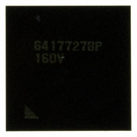
HD6417727BP160CV Renesas Electronics America, HD6417727BP160CV Datasheet - Page 987

HD6417727BP160CV
Manufacturer Part Number
HD6417727BP160CV
Description
IC SH MPU ROMLESS 240BGA
Manufacturer
Renesas Electronics America
Series
SuperH® SH7700r
Datasheet
1.HD6417727BP100CV.pdf
(1098 pages)
Specifications of HD6417727BP160CV
Core Processor
SH-3 DSP
Core Size
32-Bit
Speed
160MHz
Connectivity
FIFO, SCI, SIO, SmartCard, USB
Peripherals
DMA, LCD, POR, WDT
Number Of I /o
104
Program Memory Type
ROMless
Ram Size
32K x 8
Voltage - Supply (vcc/vdd)
1.7 V ~ 2.05 V
Data Converters
A/D 6x10b; D/A 2x8b
Oscillator Type
Internal
Operating Temperature
-20°C ~ 75°C
Package / Case
240-BGA
Package
240CSP
Family Name
SuperH
Maximum Speed
160 MHz
Operating Supply Voltage
1.8|3.3 V
Data Bus Width
32 Bit
Number Of Programmable I/os
104
Interface Type
SCI/USB
On-chip Adc
6-chx10-bit
On-chip Dac
2-chx8-bit
Number Of Timers
4
Lead Free Status / RoHS Status
Lead free / RoHS Compliant
Eeprom Size
-
Program Memory Size
-
Available stocks
Company
Part Number
Manufacturer
Quantity
Price
Company:
Part Number:
HD6417727BP160CV
Manufacturer:
LITEON
Quantity:
46 000
Company:
Part Number:
HD6417727BP160CV
Manufacturer:
Renesas Electronics America
Quantity:
10 000
- Current page: 987 of 1098
- Download datasheet (7Mb)
Table 32.1 shows the absolute maximum ratings.
32.1
Table 32.1 Absolute Maximum Ratings
Item
Power supply voltage (I/O)
Power supply voltage (internal) Vcc
Input voltage (except port L)
Input voltage (port L)
Analog power-supply voltage
USB power-supply voltage
Analog input voltage
Operating temperature
Storage temperature
Caution: Operating the chip in excess of the absolute maximum rating may result in permanent
damage.
• Order of turning on 1.9 V power (Vcc, Vcc-PLL1, Vcc-PLL2, Vcc-RTC) and 3.3 V power
(VccQ, AVcc, AVcc_USB):
1. First turn on the 3.3 V power, then turn on the 1.9 V power within 1 ms. This interval
2. Until Voltage is applied to all power supplies, a low level is input at the RESETP pin and, a
3. The state of pins MD5 to MD0 should be established after power supply startup and
Waveforms at power-on are shown in the following figure 32.1.
should be as short as possible.
maximum of 4 CKIO clock cycles have been generated, internal circuits remain unsettled,
and so pin states are also undefined. The system design must ensure that these undefined
states do not cause erroneous system operation.
Note that the RESETP pin will not accept low level input while the CA pin is low level.
maintained until after the RESETP pin is negated. Read-in of pins MD5 to MD0 is always
performed while the RESETP pin is asserted.
Absolute Maximum Ratings
Section 32 Electrical Characteristics
Topr
Symbol
VccQ
Vcc – PLL1
Vcc – PLL2
Vcc – RTC
Vin
Vin
AVcc
AVcc_USB
V
Tstr
AN
Rating
–0.3 to 4.2
–0.3 to 2.5
–0.3 to VccQ + 0.3
–0.3 to AVcc + 0.3
–0.3 to 4.6
–0.3 to 4.2
–0.3 to AVcc + 0.3
–20 to 75
–55 to 125
Rev.6.00 Mar. 27, 2009 Page 929 of 1036
Section 32 Electrical Characteristics
REJ09B0254-0600
Unit
V
V
V
V
V
V
V
°C
°C
Related parts for HD6417727BP160CV
Image
Part Number
Description
Manufacturer
Datasheet
Request
R

Part Number:
Description:
KIT STARTER FOR M16C/29
Manufacturer:
Renesas Electronics America
Datasheet:

Part Number:
Description:
KIT STARTER FOR R8C/2D
Manufacturer:
Renesas Electronics America
Datasheet:

Part Number:
Description:
R0K33062P STARTER KIT
Manufacturer:
Renesas Electronics America
Datasheet:

Part Number:
Description:
KIT STARTER FOR R8C/23 E8A
Manufacturer:
Renesas Electronics America
Datasheet:

Part Number:
Description:
KIT STARTER FOR R8C/25
Manufacturer:
Renesas Electronics America
Datasheet:

Part Number:
Description:
KIT STARTER H8S2456 SHARPE DSPLY
Manufacturer:
Renesas Electronics America
Datasheet:

Part Number:
Description:
KIT STARTER FOR R8C38C
Manufacturer:
Renesas Electronics America
Datasheet:

Part Number:
Description:
KIT STARTER FOR R8C35C
Manufacturer:
Renesas Electronics America
Datasheet:

Part Number:
Description:
KIT STARTER FOR R8CL3AC+LCD APPS
Manufacturer:
Renesas Electronics America
Datasheet:

Part Number:
Description:
KIT STARTER FOR RX610
Manufacturer:
Renesas Electronics America
Datasheet:

Part Number:
Description:
KIT STARTER FOR R32C/118
Manufacturer:
Renesas Electronics America
Datasheet:

Part Number:
Description:
KIT DEV RSK-R8C/26-29
Manufacturer:
Renesas Electronics America
Datasheet:

Part Number:
Description:
KIT STARTER FOR SH7124
Manufacturer:
Renesas Electronics America
Datasheet:

Part Number:
Description:
KIT STARTER FOR H8SX/1622
Manufacturer:
Renesas Electronics America
Datasheet:

Part Number:
Description:
KIT DEV FOR SH7203
Manufacturer:
Renesas Electronics America
Datasheet:


