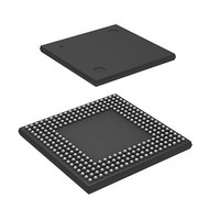
HD6417750SBP200 Renesas Electronics America, HD6417750SBP200 Datasheet - Page 1147

HD6417750SBP200
Manufacturer Part Number
HD6417750SBP200
Description
IC SUPERH MPU ROMLESS 256BGA
Manufacturer
Renesas Electronics America
Series
SuperH® SH7750r
Datasheet
1.D6417750RBP240DV.pdf
(1164 pages)
Specifications of HD6417750SBP200
Core Processor
SH-4
Core Size
32-Bit
Speed
200MHz
Connectivity
EBI/EMI, FIFO, SCI, SmartCard
Peripherals
DMA, POR, WDT
Number Of I /o
28
Program Memory Type
ROMless
Ram Size
24K x 8
Voltage - Supply (vcc/vdd)
1.8 V ~ 2.07 V
Oscillator Type
External
Operating Temperature
-20°C ~ 75°C
Package / Case
256-BGA
Lead Free Status / RoHS Status
Contains lead / RoHS non-compliant
Eeprom Size
-
Program Memory Size
-
Data Converters
-
Available stocks
Company
Part Number
Manufacturer
Quantity
Price
Part Number:
HD6417750SBP200
Manufacturer:
RENESAS/瑞萨
Quantity:
20 000
- Current page: 1147 of 1164
- Download datasheet (7Mb)
H.1
1. Supply power to power supply V
2. Perform input to the signal lines (RESET, MRESET, MD0 to MD10, external clock, etc.) after
3. It is recommended to apply power first to power supply V
4. In addition to 1., 2., and 3. above, also observe the stipulations in H.3. Furthermore:
H.2
1. Power off power supply V
2. There are no timing restrictions for the RESET and MRESET signal lines at power-off.
3. Cut off the input signal level for signal lines other than RESET and MRESET in the same
4. It is recommended to first power off power supply V
5. In addition to 1., 2., 3., and 4. above, also observe the stipulations in H.3. Furthermore:
or at the same time power is supplied to V
supplied to V
⎯ Drive the RESET signal low when power is first supplied to V
⎯ Input a high-level MRESET signal in the same sequence as power supply V
⎯ There are no time restrictions on the power-on sequence for power supply V
⎯ When the LSI is mounted on a board and connected to other elements, ensure that –0.3 V <
sequence as power supply V
⎯ There are no time restrictions on the power-off sequence for power supply V
is first supplied to V
supply V
recommended that the power-on sequence be completed in as short a time as possible.
Vin < V
supply V
operation voltage range (V
H.2. The product may be damaged if this time limit is exceeded. It is recommended that the
power-on sequence be completed in as short a time as possible.
supply V
recommended that the power-off sequence be completed in as short a time as possible.
Appendix H Power-On and Power-Off Procedures
Power-On Stipulations
Power-Off Stipulations
DDQ
DD
DD
DD
DDQ
with regard to the LSI alone. Refer to figure H.1. Nevertheless, it is
+ 0.3 V. In addition, the time limit for the rise of power supply V
from GND (0 V) to above the minimum values in the LSI’s guaranteed
with regard to the LSI alone. Refer to figure H.1. Nevertheless, it is
could damage the product.
DDQ
DDQ
.
DDQ
and I/O, RTC, CPG, PLL1, and PLL2 simultaneously.
DDQ
.
DDQ
(min.) and V
and to I/O, RTC, CPG, PLL1, and PLL2 simultaneously.
DDQ
Appendix H Power-On and Power-Off Procedures
. Applying input to signal lines before power is
DD
(min.)) is 100 ms (max.), as shown in figure
Rev.7.00 Oct. 10, 2008 Page 1061 of 1074
DD
and then power supply V
DDQ
and then to power supply V
DDQ
.
REJ09B0366-0700
DDQ
DDQ
DDQ
DDQ
DDQ
when power
.
and power
and power
and power
DD
.
Related parts for HD6417750SBP200
Image
Part Number
Description
Manufacturer
Datasheet
Request
R

Part Number:
Description:
KIT STARTER FOR M16C/29
Manufacturer:
Renesas Electronics America
Datasheet:

Part Number:
Description:
KIT STARTER FOR R8C/2D
Manufacturer:
Renesas Electronics America
Datasheet:

Part Number:
Description:
R0K33062P STARTER KIT
Manufacturer:
Renesas Electronics America
Datasheet:

Part Number:
Description:
KIT STARTER FOR R8C/23 E8A
Manufacturer:
Renesas Electronics America
Datasheet:

Part Number:
Description:
KIT STARTER FOR R8C/25
Manufacturer:
Renesas Electronics America
Datasheet:

Part Number:
Description:
KIT STARTER H8S2456 SHARPE DSPLY
Manufacturer:
Renesas Electronics America
Datasheet:

Part Number:
Description:
KIT STARTER FOR R8C38C
Manufacturer:
Renesas Electronics America
Datasheet:

Part Number:
Description:
KIT STARTER FOR R8C35C
Manufacturer:
Renesas Electronics America
Datasheet:

Part Number:
Description:
KIT STARTER FOR R8CL3AC+LCD APPS
Manufacturer:
Renesas Electronics America
Datasheet:

Part Number:
Description:
KIT STARTER FOR RX610
Manufacturer:
Renesas Electronics America
Datasheet:

Part Number:
Description:
KIT STARTER FOR R32C/118
Manufacturer:
Renesas Electronics America
Datasheet:

Part Number:
Description:
KIT DEV RSK-R8C/26-29
Manufacturer:
Renesas Electronics America
Datasheet:

Part Number:
Description:
KIT STARTER FOR SH7124
Manufacturer:
Renesas Electronics America
Datasheet:

Part Number:
Description:
KIT STARTER FOR H8SX/1622
Manufacturer:
Renesas Electronics America
Datasheet:

Part Number:
Description:
KIT DEV FOR SH7203
Manufacturer:
Renesas Electronics America
Datasheet:


