HD6417750SBP200 Renesas Electronics America, HD6417750SBP200 Datasheet - Page 25
HD6417750SBP200
Manufacturer Part Number
HD6417750SBP200
Description
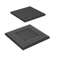
IC SUPERH MPU ROMLESS 256BGA
Manufacturer
Renesas Electronics America
Series
SuperH® SH7750r
Datasheet
1.D6417750RBP240DV.pdf
(1164 pages)
Specifications of HD6417750SBP200
Core Processor
SH-4
Core Size
32-Bit
Speed
200MHz
Connectivity
EBI/EMI, FIFO, SCI, SmartCard
Peripherals
DMA, POR, WDT
Number Of I /o
28
Program Memory Type
ROMless
Ram Size
24K x 8
Voltage - Supply (vcc/vdd)
1.8 V ~ 2.07 V
Oscillator Type
External
Operating Temperature
-20°C ~ 75°C
Package / Case
256-BGA
Lead Free Status / RoHS Status
Contains lead / RoHS non-compliant
Eeprom Size
-
Program Memory Size
-
Data Converters
-
Available stocks
Company
Part Number
Manufacturer
Quantity
Price

Part Number:
HD6417750SBP200
Manufacturer:
RENESAS/瑞萨
Quantity:
20 000


Item
13.3.8 MPX Interface
Figure 13.68 MPX
Interface Timing 11
(Burst Write Cycle, AnW
= 0, No External Wait,
Bus Width: 32 Bits,
Transfer Data Size: 64
Bits)
Figure 13.69 MPX
Interface Timing 12
(Burst Write Cycle, AnW
= 1, One External Wait
Inserted, Bus Width: 32
Bits, Transfer Data Size:
64 Bits)
13.3.16 Notes on
Usage
Synchronous DRAM
Mode Register Setting
(SH7750, SH7750S
Only):
BSREQ Output in
Partial-Sharing Master
Mode
14.2.1 DMA Source
Address Registers 0–3
(SAR0–SAR3)
14.2.4 DMA Channel
Control Registers 0−3
(CHCR0−CHCR3)
Bits 13 and 12⎯Source
Address Mode 1 and 0
(SM1, SM0):
Page
523
524
543
543, 544 Newly added
552
560
Revision (See Manual for Details)
Title amended
Title amended
Notes amended
3. If synchronous DRAM mode register setting is performed
immediately following write access to the on-chip peripheral
modules*
cannot be guaranteed. Note that following power-on,
synchronous DRAM mode register settings should be
performed before accessing synchronous DRAM. After making
mode register settings, do not change them.
Description deleted
When transfer is performed from memory to an external device
with DACK in DDT mode, DTR format [31:0] is set in SAR0
[31:0]. For details, see Data Transfer Request Format in section
14.5.2, Pin in DDT Mode.
Description amended
These bits specify incrementing/decrementing of the DMA
transfer source address. The specification of these bits is
ignored when data is transferred from an external device to
external memory in single address mode. For channel 0, in
DDT mode these bits are set to SM1 = 0 and SM0 = 1 with the
DTR format.
2
, the values written to the on-chip peripheral modules
Rev.7.00 Oct. 10, 2008 Page xxiii of lxxxiv
REJ09B0366-0700
Related parts for HD6417750SBP200
Image
Part Number
Description
Manufacturer
Datasheet
Request
R

Part Number:
Description:
KIT STARTER FOR M16C/29
Manufacturer:
Renesas Electronics America
Datasheet:

Part Number:
Description:
KIT STARTER FOR R8C/2D
Manufacturer:
Renesas Electronics America
Datasheet:

Part Number:
Description:
R0K33062P STARTER KIT
Manufacturer:
Renesas Electronics America
Datasheet:

Part Number:
Description:
KIT STARTER FOR R8C/23 E8A
Manufacturer:
Renesas Electronics America
Datasheet:

Part Number:
Description:
KIT STARTER FOR R8C/25
Manufacturer:
Renesas Electronics America
Datasheet:

Part Number:
Description:
KIT STARTER H8S2456 SHARPE DSPLY
Manufacturer:
Renesas Electronics America
Datasheet:

Part Number:
Description:
KIT STARTER FOR R8C38C
Manufacturer:
Renesas Electronics America
Datasheet:

Part Number:
Description:
KIT STARTER FOR R8C35C
Manufacturer:
Renesas Electronics America
Datasheet:

Part Number:
Description:
KIT STARTER FOR R8CL3AC+LCD APPS
Manufacturer:
Renesas Electronics America
Datasheet:
Part Number:
Description:
KIT STARTER FOR RX610
Manufacturer:
Renesas Electronics America
Datasheet:

Part Number:
Description:
KIT STARTER FOR R32C/118
Manufacturer:
Renesas Electronics America
Datasheet:

Part Number:
Description:
KIT DEV RSK-R8C/26-29
Manufacturer:
Renesas Electronics America
Datasheet:

Part Number:
Description:
KIT STARTER FOR SH7124
Manufacturer:
Renesas Electronics America
Datasheet:

Part Number:
Description:
KIT STARTER FOR H8SX/1622
Manufacturer:
Renesas Electronics America
Datasheet:

Part Number:
Description:
KIT DEV FOR SH7203
Manufacturer:
Renesas Electronics America
Datasheet: