HD6417750SBP200 Renesas Electronics America, HD6417750SBP200 Datasheet - Page 226
HD6417750SBP200
Manufacturer Part Number
HD6417750SBP200
Description
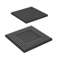
IC SUPERH MPU ROMLESS 256BGA
Manufacturer
Renesas Electronics America
Series
SuperH® SH7750r
Datasheet
1.D6417750RBP240DV.pdf
(1164 pages)
Specifications of HD6417750SBP200
Core Processor
SH-4
Core Size
32-Bit
Speed
200MHz
Connectivity
EBI/EMI, FIFO, SCI, SmartCard
Peripherals
DMA, POR, WDT
Number Of I /o
28
Program Memory Type
ROMless
Ram Size
24K x 8
Voltage - Supply (vcc/vdd)
1.8 V ~ 2.07 V
Oscillator Type
External
Operating Temperature
-20°C ~ 75°C
Package / Case
256-BGA
Lead Free Status / RoHS Status
Contains lead / RoHS non-compliant
Eeprom Size
-
Program Memory Size
-
Data Converters
-
Available stocks
Company
Part Number
Manufacturer
Quantity
Price

Part Number:
HD6417750SBP200
Manufacturer:
RENESAS/瑞萨
Quantity:
20 000


Section 4 Caches
2. OC address array write (non-associative)
3. OC address array write (associative)
Rev.7.00 Oct. 10, 2008 Page 140 of 1074
REJ09B0366-0700
Legend:
V: Validity bit
U: Dirty bit
A: Association bit
Address field
The tag, U bit, and V bit specified in the data field are written to the OC entry corresponding to
the way and the entry set in the address field. The A bit in the address field should be cleared
to 0.
When a write is performed to a cache line for which the U bit and V bit are both 1, after write-
back of that cache line, the tag, U bit, and V bit specified in the data field are written.
When a write is performed with the A bit in the address field set to 1, the tag for each of the
ways stored in the entry specified in the address field is compared with the tag specified in the
data field. The way number set by bit [14] is not used. If the MMU is enabled at this time,
comparison is performed after the virtual address specified by data field bits [31:10] has been
translated to a physical address using the UTLB. If the addresses match and the V bit for that
way is 1, the U bit and V bit specified in the data field are written into the OC entry. This
operation is used to invalidate a specific OC entry. In other cases, no operation is performed. If
the OC entry U bit is 1, and 0 is written to the V bit or to the U bit, write-back is performed. If
an UTLB miss occurs during address translation, or the comparison shows a mismatch, an
exception is not generated, no operation is performed, and the write is not executed. If a data
TLB multiple hit exception occurs during address translation, processing switches to the data
TLB multiple hit exception handling routine.
Data field
: Reserved bits (0 write value, undefined read value)
31
31
1 1 1 1 0 1 0 0
Figure 4.14 Memory-Mapped OC Address Array
24
23
Tag
15
Way
14
13
10 9
Entry
5 4 3 2 1 0
A
2
U
1 0
V
Related parts for HD6417750SBP200
Image
Part Number
Description
Manufacturer
Datasheet
Request
R

Part Number:
Description:
KIT STARTER FOR M16C/29
Manufacturer:
Renesas Electronics America
Datasheet:

Part Number:
Description:
KIT STARTER FOR R8C/2D
Manufacturer:
Renesas Electronics America
Datasheet:

Part Number:
Description:
R0K33062P STARTER KIT
Manufacturer:
Renesas Electronics America
Datasheet:

Part Number:
Description:
KIT STARTER FOR R8C/23 E8A
Manufacturer:
Renesas Electronics America
Datasheet:

Part Number:
Description:
KIT STARTER FOR R8C/25
Manufacturer:
Renesas Electronics America
Datasheet:

Part Number:
Description:
KIT STARTER H8S2456 SHARPE DSPLY
Manufacturer:
Renesas Electronics America
Datasheet:

Part Number:
Description:
KIT STARTER FOR R8C38C
Manufacturer:
Renesas Electronics America
Datasheet:

Part Number:
Description:
KIT STARTER FOR R8C35C
Manufacturer:
Renesas Electronics America
Datasheet:

Part Number:
Description:
KIT STARTER FOR R8CL3AC+LCD APPS
Manufacturer:
Renesas Electronics America
Datasheet:
Part Number:
Description:
KIT STARTER FOR RX610
Manufacturer:
Renesas Electronics America
Datasheet:

Part Number:
Description:
KIT STARTER FOR R32C/118
Manufacturer:
Renesas Electronics America
Datasheet:

Part Number:
Description:
KIT DEV RSK-R8C/26-29
Manufacturer:
Renesas Electronics America
Datasheet:

Part Number:
Description:
KIT STARTER FOR SH7124
Manufacturer:
Renesas Electronics America
Datasheet:

Part Number:
Description:
KIT STARTER FOR H8SX/1622
Manufacturer:
Renesas Electronics America
Datasheet:

Part Number:
Description:
KIT DEV FOR SH7203
Manufacturer:
Renesas Electronics America
Datasheet: