HD6417750SBP200 Renesas Electronics America, HD6417750SBP200 Datasheet - Page 20
HD6417750SBP200
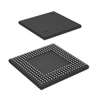
Manufacturer Part Number
HD6417750SBP200
Description
IC SUPERH MPU ROMLESS 256BGA
Manufacturer
Renesas Electronics America
Series
SuperH® SH7750r
Datasheet
1.D6417750RBP240DV.pdf
(1164 pages)
Specifications of HD6417750SBP200
Core Processor
SH-4
Core Size
32-Bit
Speed
200MHz
Connectivity
EBI/EMI, FIFO, SCI, SmartCard
Peripherals
DMA, POR, WDT
Number Of I /o
28
Program Memory Type
ROMless
Ram Size
24K x 8
Voltage - Supply (vcc/vdd)
1.8 V ~ 2.07 V
Oscillator Type
External
Operating Temperature
-20°C ~ 75°C
Package / Case
256-BGA
Lead Free Status / RoHS Status
Contains lead / RoHS non-compliant
Eeprom Size
-
Program Memory Size
-
Data Converters
-
Available stocks
Company
Part Number
Manufacturer
Quantity
Price

Part Number:
HD6417750SBP200
Manufacturer:
RENESAS/瑞萨
Quantity:
20 000


Rev.7.00 Oct. 10, 2008 Page xviii of lxxxiv
REJ09B0366-0700
Item
13.2.8 Memory Control
Register (MCR)
Bit 31—RAS Down
(RASD):
Bits 29 to 27—RAS
Precharge Time at End
of Refresh (TRC2–
TRC0)
Bits 21 to 19—RAS
Precharge Period
(TPC2–TPC0):
Bits 15 to 13—Write
Precharge Delay
(TRWL2–TRWL0):
Bits 12 to 10—CAS-
Before-RAS Refresh
RAS Assertion Period
(TRAS2–TRAS0):
Page
402
402
403
404
405
Revision (See Manual for Details)
Description and table amended
Do not set RAS down mode in slave mode or partial-sharing
mode, or when areas 2 and 3 are both designated as
synchronous DRAM interface. See Connecting a 128-Mbit/256-
Mbit Synchronous DRAM with 64-bit Bus Width (SH7750R
Only): in section 13.3.5, Synchronous DRAM Interface.
Bit 31: RASD
0
Note added
Note: For setting values and the period during which no
Description amended and note added
When the DRAM interface is selected, these bits specify the
minimum number of cycles until RAS is asserted again after
being negated. When the synchronous DRAM interface is
selected, these bits specify the minimum number of cycles until
the next bank active command
Note: For setting values and the period during which no
Description amended and note added
After a write cycle, the next active command is not issued for a
period equivalent to the
TRWL[2:0] bits.* ...
Note: * For setting values and the period during which no
Description amended and note added
When the DRAM interface is set, these bits set the RAS
assertion period in CAS-before-RAS refreshing. When the
synchronous DRAM interface is set, the bank active command
is not issued for the period set by the TRC[2:0]* and TRAS[2:0]
bits after an auto-refresh command is issued.
Note: For setting values and the period during which no
command is issued, see 22.3.3, Bus Timing.
command is issued, see 22.3.3, Bus Timing.
command is issued, see 22.3.3, Bus Timing.
command is issued, see 22.3.3, Bus Timing.
Description
Auto-precharge mode
setting values of the TPC[2:0] and
after precharging.
(Initial value)
Related parts for HD6417750SBP200
Image
Part Number
Description
Manufacturer
Datasheet
Request
R

Part Number:
Description:
KIT STARTER FOR M16C/29
Manufacturer:
Renesas Electronics America
Datasheet:

Part Number:
Description:
KIT STARTER FOR R8C/2D
Manufacturer:
Renesas Electronics America
Datasheet:

Part Number:
Description:
R0K33062P STARTER KIT
Manufacturer:
Renesas Electronics America
Datasheet:

Part Number:
Description:
KIT STARTER FOR R8C/23 E8A
Manufacturer:
Renesas Electronics America
Datasheet:

Part Number:
Description:
KIT STARTER FOR R8C/25
Manufacturer:
Renesas Electronics America
Datasheet:

Part Number:
Description:
KIT STARTER H8S2456 SHARPE DSPLY
Manufacturer:
Renesas Electronics America
Datasheet:

Part Number:
Description:
KIT STARTER FOR R8C38C
Manufacturer:
Renesas Electronics America
Datasheet:

Part Number:
Description:
KIT STARTER FOR R8C35C
Manufacturer:
Renesas Electronics America
Datasheet:

Part Number:
Description:
KIT STARTER FOR R8CL3AC+LCD APPS
Manufacturer:
Renesas Electronics America
Datasheet:
Part Number:
Description:
KIT STARTER FOR RX610
Manufacturer:
Renesas Electronics America
Datasheet:

Part Number:
Description:
KIT STARTER FOR R32C/118
Manufacturer:
Renesas Electronics America
Datasheet:

Part Number:
Description:
KIT DEV RSK-R8C/26-29
Manufacturer:
Renesas Electronics America
Datasheet:

Part Number:
Description:
KIT STARTER FOR SH7124
Manufacturer:
Renesas Electronics America
Datasheet:

Part Number:
Description:
KIT STARTER FOR H8SX/1622
Manufacturer:
Renesas Electronics America
Datasheet:

Part Number:
Description:
KIT DEV FOR SH7203
Manufacturer:
Renesas Electronics America
Datasheet: