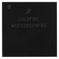
MCF5282CVF80 Freescale Semiconductor, MCF5282CVF80 Datasheet - Page 225

MCF5282CVF80
Manufacturer Part Number
MCF5282CVF80
Description
IC MPU 32BIT 66MHZ 256-MAPBGA
Manufacturer
Freescale Semiconductor
Series
MCF528xr
Datasheet
1.MCF5216CVM66J.pdf
(766 pages)
Specifications of MCF5282CVF80
Core Processor
Coldfire V2
Core Size
32-Bit
Speed
80MHz
Connectivity
CAN, EBI/EMI, Ethernet, I²C, SPI, UART/USART
Peripherals
DMA, LVD, POR, PWM, WDT
Number Of I /o
142
Program Memory Size
512KB (512K x 8)
Program Memory Type
FLASH
Ram Size
64K x 8
Voltage - Supply (vcc/vdd)
2.7 V ~ 3.6 V
Data Converters
A/D 8x10b
Oscillator Type
External
Operating Temperature
-40°C ~ 85°C
Package / Case
256-MAPBGA
Controller Family/series
ColdFire
Ram Memory Size
64KB
Embedded Interface Type
CAN, I2C, SPI, UART
No. Of Pwm Channels
8
Digital Ic Case Style
MAPBGA
Rohs Compliant
No
Package
256MA-BGA
Device Core
ColdFire
Family Name
MCF528x
Maximum Speed
80 MHz
Operating Supply Voltage
3.3 V
Data Bus Width
32 Bit
Number Of Programmable I/os
150
Interface Type
CAN/Ethernet/I2C/QSPI/UART
On-chip Adc
8-chx10-bit
Number Of Timers
12
Lead Free Status / RoHS Status
Contains lead / RoHS non-compliant
Eeprom Size
-
Available stocks
Company
Part Number
Manufacturer
Quantity
Price
Company:
Part Number:
MCF5282CVF80
Manufacturer:
FREESCALE
Quantity:
12 388
Company:
Part Number:
MCF5282CVF80
Manufacturer:
Freescale Semiconductor
Quantity:
10 000
Company:
Part Number:
MCF5282CVF80J
Manufacturer:
Freescale Semiconductor
Quantity:
10 000
- Current page: 225 of 766
- Download datasheet (9Mb)
Chapter 13
External Interface Module (EIM)
This chapter describes data-transfer operations, error conditions, and reset operations.
“Synchronous DRAM Controller
13.1
The following list summarizes bus operation features:
13.2
Table 13-1
Freescale Semiconductor
•
•
•
•
•
Up to 24 bits of address and 32 bits of data
Access 8-, 16-, and 32-bit data port sizes
Generates byte, word, longword, and line-size transfers
Burst and burst-inhibited transfer support
Optional internal termination for external bus cycles
Features
Bus and Control Signals
summarizes the bus signals described in
1
These signals change after the falling edge. In the Electrical Specifications, these signals are
specified off of the rising edge because CLKIN is squared up internally.
Unless otherwise noted, in this chapter, “clock” refers to the CLKOUT used
for the bus.
Signal Name
CS[6:0]
SIZ[1:0]
A[23:0]
D[31:0]
OE
BS
R/W
TIP
TS
TA
1
1
1
MCF5282 and MCF5216 ColdFire Microcontroller User’s Manual, Rev. 3
Address bus
Byte selects
Chip selects
Data bus
Output enable
Read/write
Transfer size
Transfer acknowledge
Transfer in progress
Transfer start
Table 13-1. ColdFire Bus Signal Summary
Module,” describes DRAM cycles.
Description
NOTE
Chapter 14, “Signal
I/O
I/O
O
O
O
O
O
O
O
O
I
Descriptions”.
Rising
Falling
Falling
Rising
Falling
Rising
Rising
Rising
Rising
Rising
CLKOUT Edge
Chapter 15,
13-1
Related parts for MCF5282CVF80
Image
Part Number
Description
Manufacturer
Datasheet
Request
R
Part Number:
Description:
Mcf5282 And Mcf5216 Coldfire Microcontroller User�s Manual
Manufacturer:
Freescale Semiconductor, Inc
Datasheet:
Part Number:
Description:
Manufacturer:
Freescale Semiconductor, Inc
Datasheet:
Part Number:
Description:
Manufacturer:
Freescale Semiconductor, Inc
Datasheet:
Part Number:
Description:
Manufacturer:
Freescale Semiconductor, Inc
Datasheet:
Part Number:
Description:
Manufacturer:
Freescale Semiconductor, Inc
Datasheet:
Part Number:
Description:
Manufacturer:
Freescale Semiconductor, Inc
Datasheet:
Part Number:
Description:
Manufacturer:
Freescale Semiconductor, Inc
Datasheet:
Part Number:
Description:
Manufacturer:
Freescale Semiconductor, Inc
Datasheet:
Part Number:
Description:
Manufacturer:
Freescale Semiconductor, Inc
Datasheet:
Part Number:
Description:
Manufacturer:
Freescale Semiconductor, Inc
Datasheet:
Part Number:
Description:
Manufacturer:
Freescale Semiconductor, Inc
Datasheet:
Part Number:
Description:
Manufacturer:
Freescale Semiconductor, Inc
Datasheet:
Part Number:
Description:
Manufacturer:
Freescale Semiconductor, Inc
Datasheet:
Part Number:
Description:
Manufacturer:
Freescale Semiconductor, Inc
Datasheet:
Part Number:
Description:
Manufacturer:
Freescale Semiconductor, Inc
Datasheet:


