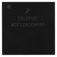
MCF5282CVF80 Freescale Semiconductor, MCF5282CVF80 Datasheet - Page 286

MCF5282CVF80
Manufacturer Part Number
MCF5282CVF80
Description
IC MPU 32BIT 66MHZ 256-MAPBGA
Manufacturer
Freescale Semiconductor
Series
MCF528xr
Datasheet
1.MCF5216CVM66J.pdf
(766 pages)
Specifications of MCF5282CVF80
Core Processor
Coldfire V2
Core Size
32-Bit
Speed
80MHz
Connectivity
CAN, EBI/EMI, Ethernet, I²C, SPI, UART/USART
Peripherals
DMA, LVD, POR, PWM, WDT
Number Of I /o
142
Program Memory Size
512KB (512K x 8)
Program Memory Type
FLASH
Ram Size
64K x 8
Voltage - Supply (vcc/vdd)
2.7 V ~ 3.6 V
Data Converters
A/D 8x10b
Oscillator Type
External
Operating Temperature
-40°C ~ 85°C
Package / Case
256-MAPBGA
Controller Family/series
ColdFire
Ram Memory Size
64KB
Embedded Interface Type
CAN, I2C, SPI, UART
No. Of Pwm Channels
8
Digital Ic Case Style
MAPBGA
Rohs Compliant
No
Package
256MA-BGA
Device Core
ColdFire
Family Name
MCF528x
Maximum Speed
80 MHz
Operating Supply Voltage
3.3 V
Data Bus Width
32 Bit
Number Of Programmable I/os
150
Interface Type
CAN/Ethernet/I2C/QSPI/UART
On-chip Adc
8-chx10-bit
Number Of Timers
12
Lead Free Status / RoHS Status
Contains lead / RoHS non-compliant
Eeprom Size
-
Available stocks
Company
Part Number
Manufacturer
Quantity
Price
Company:
Part Number:
MCF5282CVF80
Manufacturer:
FREESCALE
Quantity:
12 388
Company:
Part Number:
MCF5282CVF80
Manufacturer:
Freescale Semiconductor
Quantity:
10 000
Company:
Part Number:
MCF5282CVF80J
Manufacturer:
Freescale Semiconductor
Quantity:
10 000
- Current page: 286 of 766
- Download datasheet (9Mb)
Synchronous DRAM Controller Module
Note that in synchronous operation, burst mode and address incrementing during burst cycles are
controlled by the DRAM controller. Thus, instead of the SDRAM enabling its internal burst incrementing
capability, the processor controls this function. This means that the burst function that is enabled in the
mode register of SDRAMs must be disabled when interfacing to the processor.
Figure 15-6
delay (t
data out), this value is also 2 system clock cycles. Notice that
A
Figure 15-7
SRAS-to-SCAS delay (t
and a burst write cycle completes two cycles sooner than a burst read cycle with the same t
bus cycle is initiated sooner, but cannot begin an SDRAM cycle until the precharge-to-
completes.
15-14
PALL
SDRAM_CS[0] or [1]
RCD
command is executed one cycle after the last data transfer.
) of 2 system clock cycles. Because t
CLKOUT
DRAMW
shows a burst read operation. In this example, DACR[CASL] = 01 for an SRAS-to-SCAS
shows the burst write operation. In this example, DACR[CASL] = 01, which creates an
A[23:0]
D[31:0]
BS[3:0]
SRAS
SCAS
RCD
MCF5282 and MCF5216 ColdFire Microcontroller User’s Manual, Rev. 3
t
RCD
ACTV
Row
) of 2 system clock cycles. Note that data is available upon SCAS assertion
= 2
Figure 15-6. Burst Read SDRAM Access
NOP
Column Column Column
READ
t
CASL
RCD
READ
= 2
is equal to the read CAS latency (SCAS assertion to
READ
NOP
Column
s are executed until the last data is read.
READ
NOP
t
EP
NOP
Freescale Semiconductor
PALL
RCD.
ACTV
The next
delay
Related parts for MCF5282CVF80
Image
Part Number
Description
Manufacturer
Datasheet
Request
R
Part Number:
Description:
Mcf5282 And Mcf5216 Coldfire Microcontroller User�s Manual
Manufacturer:
Freescale Semiconductor, Inc
Datasheet:
Part Number:
Description:
Manufacturer:
Freescale Semiconductor, Inc
Datasheet:
Part Number:
Description:
Manufacturer:
Freescale Semiconductor, Inc
Datasheet:
Part Number:
Description:
Manufacturer:
Freescale Semiconductor, Inc
Datasheet:
Part Number:
Description:
Manufacturer:
Freescale Semiconductor, Inc
Datasheet:
Part Number:
Description:
Manufacturer:
Freescale Semiconductor, Inc
Datasheet:
Part Number:
Description:
Manufacturer:
Freescale Semiconductor, Inc
Datasheet:
Part Number:
Description:
Manufacturer:
Freescale Semiconductor, Inc
Datasheet:
Part Number:
Description:
Manufacturer:
Freescale Semiconductor, Inc
Datasheet:
Part Number:
Description:
Manufacturer:
Freescale Semiconductor, Inc
Datasheet:
Part Number:
Description:
Manufacturer:
Freescale Semiconductor, Inc
Datasheet:
Part Number:
Description:
Manufacturer:
Freescale Semiconductor, Inc
Datasheet:
Part Number:
Description:
Manufacturer:
Freescale Semiconductor, Inc
Datasheet:
Part Number:
Description:
Manufacturer:
Freescale Semiconductor, Inc
Datasheet:
Part Number:
Description:
Manufacturer:
Freescale Semiconductor, Inc
Datasheet:


