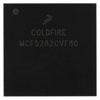
MCF5282CVF80 Freescale Semiconductor, MCF5282CVF80 Datasheet - Page 292

MCF5282CVF80
Manufacturer Part Number
MCF5282CVF80
Description
IC MPU 32BIT 66MHZ 256-MAPBGA
Manufacturer
Freescale Semiconductor
Series
MCF528xr
Datasheet
1.MCF5216CVM66J.pdf
(766 pages)
Specifications of MCF5282CVF80
Core Processor
Coldfire V2
Core Size
32-Bit
Speed
80MHz
Connectivity
CAN, EBI/EMI, Ethernet, I²C, SPI, UART/USART
Peripherals
DMA, LVD, POR, PWM, WDT
Number Of I /o
142
Program Memory Size
512KB (512K x 8)
Program Memory Type
FLASH
Ram Size
64K x 8
Voltage - Supply (vcc/vdd)
2.7 V ~ 3.6 V
Data Converters
A/D 8x10b
Oscillator Type
External
Operating Temperature
-40°C ~ 85°C
Package / Case
256-MAPBGA
Controller Family/series
ColdFire
Ram Memory Size
64KB
Embedded Interface Type
CAN, I2C, SPI, UART
No. Of Pwm Channels
8
Digital Ic Case Style
MAPBGA
Rohs Compliant
No
Package
256MA-BGA
Device Core
ColdFire
Family Name
MCF528x
Maximum Speed
80 MHz
Operating Supply Voltage
3.3 V
Data Bus Width
32 Bit
Number Of Programmable I/os
150
Interface Type
CAN/Ethernet/I2C/QSPI/UART
On-chip Adc
8-chx10-bit
Number Of Timers
12
Lead Free Status / RoHS Status
Contains lead / RoHS non-compliant
Eeprom Size
-
Available stocks
Company
Part Number
Manufacturer
Quantity
Price
Company:
Part Number:
MCF5282CVF80
Manufacturer:
FREESCALE
Quantity:
12 388
Company:
Part Number:
MCF5282CVF80
Manufacturer:
Freescale Semiconductor
Quantity:
10 000
Company:
Part Number:
MCF5282CVF80J
Manufacturer:
Freescale Semiconductor
Quantity:
10 000
- Current page: 292 of 766
- Download datasheet (9Mb)
Synchronous DRAM Controller Module
15.3.1
To interface this component to the DRAM controller, use the connection table that corresponds to a 32-bit
port size with 8 columns
Table 15-26
15.3.2
At power-up, the DCR has the following configuration if synchronous operation and SDRAM address
multiplexing are desired.
This configuration results in a value of 0x0026 for DCR, as shown in
15.3.3
As shown in
1-Mbyte partition in the SDRAM (each 16 Mbytes). The starting address of the SDRAM is 0xFF88_0000.
Continuous page mode feature is used.
15-20
Processor Pins A15
SDRAM Pins
10–9
Bits
8–0
15
14
13
12
11
Setting
(hex)
Field
Name
RTIM
NAM
COC
SDRAM Interface Configuration
DCR Initialization
DACR Initialization
RC
—
—
IS
shows the proper hardware connections.
Figure
—
15
A0
Setting
—
14
0x26
15-12, the SDRAM is programmed to access only the second 512-Kbyte block of each
00
0
0
0
0
0
NAM COC
MCF5282 and MCF5216 ColdFire Microcontroller User’s Manual, Rev. 3
A14
13
A1
Reserved.
Reserved.
Indicating SDRAM controller multiplexes address lines internally
SCKE is used as clock enable instead of command bit because user is not multiplexing
address lines externally and requires external command feed.
At power-up, allowing power self-refresh state is not appropriate because registers are being
set up.
Because t
Specification indicates auto-refresh period for 4096 rows to be 64 mS or refresh every 15.625
µs for each row, or 625 bus clocks at 40 MHz. Because DCR[RC] is incremented by 1 and
multiplied by 16, RC = (625 bus clocks/16) -1 = 38.06 = 0x38
(Table
12
Table 15-26. SDRAM Hardware Connections
A13
A2
Figure 15-11. Initialization Values for DCR
15-24). Two pins select one of four banks when the part is functional.
Table 15-27. DCR Initialization Values
RC
11
IS
A12
value is 70 ns, indicating a 3-clock refresh-to-
A3
10
A11
RTIM
A4
0000_0000_0010_0110
9
A10
A5
8
0026
A9
A6
Description
A17
A7
A18
A8
Table
A19
A9
RC
ACTV
15-27.
timing.
A10 = CMD
A20
Freescale Semiconductor
BA0
A21
0
BA1
A22
Related parts for MCF5282CVF80
Image
Part Number
Description
Manufacturer
Datasheet
Request
R
Part Number:
Description:
Mcf5282 And Mcf5216 Coldfire Microcontroller User�s Manual
Manufacturer:
Freescale Semiconductor, Inc
Datasheet:
Part Number:
Description:
Manufacturer:
Freescale Semiconductor, Inc
Datasheet:
Part Number:
Description:
Manufacturer:
Freescale Semiconductor, Inc
Datasheet:
Part Number:
Description:
Manufacturer:
Freescale Semiconductor, Inc
Datasheet:
Part Number:
Description:
Manufacturer:
Freescale Semiconductor, Inc
Datasheet:
Part Number:
Description:
Manufacturer:
Freescale Semiconductor, Inc
Datasheet:
Part Number:
Description:
Manufacturer:
Freescale Semiconductor, Inc
Datasheet:
Part Number:
Description:
Manufacturer:
Freescale Semiconductor, Inc
Datasheet:
Part Number:
Description:
Manufacturer:
Freescale Semiconductor, Inc
Datasheet:
Part Number:
Description:
Manufacturer:
Freescale Semiconductor, Inc
Datasheet:
Part Number:
Description:
Manufacturer:
Freescale Semiconductor, Inc
Datasheet:
Part Number:
Description:
Manufacturer:
Freescale Semiconductor, Inc
Datasheet:
Part Number:
Description:
Manufacturer:
Freescale Semiconductor, Inc
Datasheet:
Part Number:
Description:
Manufacturer:
Freescale Semiconductor, Inc
Datasheet:
Part Number:
Description:
Manufacturer:
Freescale Semiconductor, Inc
Datasheet:


