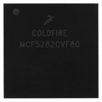
MCF5282CVF80 Freescale Semiconductor, MCF5282CVF80 Datasheet - Page 686

MCF5282CVF80
Manufacturer Part Number
MCF5282CVF80
Description
IC MPU 32BIT 66MHZ 256-MAPBGA
Manufacturer
Freescale Semiconductor
Series
MCF528xr
Datasheet
1.MCF5216CVM66J.pdf
(766 pages)
Specifications of MCF5282CVF80
Core Processor
Coldfire V2
Core Size
32-Bit
Speed
80MHz
Connectivity
CAN, EBI/EMI, Ethernet, I²C, SPI, UART/USART
Peripherals
DMA, LVD, POR, PWM, WDT
Number Of I /o
142
Program Memory Size
512KB (512K x 8)
Program Memory Type
FLASH
Ram Size
64K x 8
Voltage - Supply (vcc/vdd)
2.7 V ~ 3.6 V
Data Converters
A/D 8x10b
Oscillator Type
External
Operating Temperature
-40°C ~ 85°C
Package / Case
256-MAPBGA
Controller Family/series
ColdFire
Ram Memory Size
64KB
Embedded Interface Type
CAN, I2C, SPI, UART
No. Of Pwm Channels
8
Digital Ic Case Style
MAPBGA
Rohs Compliant
No
Package
256MA-BGA
Device Core
ColdFire
Family Name
MCF528x
Maximum Speed
80 MHz
Operating Supply Voltage
3.3 V
Data Bus Width
32 Bit
Number Of Programmable I/os
150
Interface Type
CAN/Ethernet/I2C/QSPI/UART
On-chip Adc
8-chx10-bit
Number Of Timers
12
Lead Free Status / RoHS Status
Contains lead / RoHS non-compliant
Eeprom Size
-
Available stocks
Company
Part Number
Manufacturer
Quantity
Price
Company:
Part Number:
MCF5282CVF80
Manufacturer:
FREESCALE
Quantity:
12 388
Company:
Part Number:
MCF5282CVF80
Manufacturer:
Freescale Semiconductor
Quantity:
10 000
Company:
Part Number:
MCF5282CVF80J
Manufacturer:
Freescale Semiconductor
Quantity:
10 000
- Current page: 686 of 766
- Download datasheet (9Mb)
Electrical Characteristics
33.2
Table 33-2
33-2
1
2
3
4
Junction to ambient, natural convection
Junction to ambient (@200 ft/min)
Junction to board
Junction to case
Junction to top of package
θ
Freescale recommends the use of θ
junction temperatures from exceeding the rated specification. System designers should be aware that device
junction temperatures can be significantly influenced by board layout and surrounding devices. Conformance to the
device junction temperature specification can be verified by physical measurement in the customer’s system using
the Ψ
Per JEDEC JESD51-6 with the board horizontal.
Thermal resistance between the die and the printed circuit board per JEDEC JESD51-8. Board temperature is
measured on the top surface of the board near the package.
Thermal resistance between the die and the case top surface as measured by the cold plate method (MIL SPEC-883
Method 1012.1).
JMA
Thermal Characteristics
and Ψ
jt
lists thermal resistance values.
parameter, the device power dissipation, and the method described in EIA/JESD Standard 51-2.
2
3
4
5
6
7
This device contains circuitry protecting against damage due to high static voltage or electrical
fields; however, it is advised that normal precautions be taken to avoid application of any
voltages higher than maximum-rated voltages to this high-impedance circuit. Reliability of
operation is enhanced if unused inputs are tied to an appropriate logic voltage level (e.g., either
V
Not applicable for MCF5280.
Input must be current limited to the value specified. To determine the value of the required
current-limiting resistor, calculate resistance values for positive and negative clamp voltages,
then use the larger of the two values. 6.0V voltage excludes XTAL and EXTAL pads.
All functional non-supply pins are internally clamped to V
Power supply must maintain regulation within operating V
operating maximum current conditions. If positive injection current (V
I
out of regulation. Insure external V
current. This will be the greatest risk when the MCU is not consuming power (ex; no
clock).Power supply must maintain regulation within operating V
and operating maximum current conditions.
All ESD testing methodology is in conformity with CDF-AEC-Q100 Stress Test Qualification for
Automotive Grade Integrated Circuits.
DD
jt
SS
parameters are simulated in accordance with EIA/JESD Standard 51-2 for natural convection.
, the injection current may flow out of V
or V
DD
).
MCF5282 and MCF5216 ColdFire Microcontroller User’s Manual, Rev. 3
It is crucial during power-up that V
exceeds V
diode devices between the two voltage domains,
and violating this rule can lead to a latch-up
condition.
Characteristic
Table 33-2. Thermal Characteristics
JA
and power dissipation specifications in the system design to prevent device
DDH
DD
by more than ≈0.3 V. There are
Four layer board (2s2p)
Four layer board (2s2p)
Natural convection
load will shunt current greater than maximum injection
NOTE
DD
and could result in external power supply going
SS
DD
and V
range during instantaneous and
DD
DD
DD
range during instantaneous
Symbol
.
never
in
θ
θ
θ
θ
Ψ
JMA
JMA
> V
JB
JC
jt
DD
) is greater than
Value
26
23
2
15
10
Freescale Semiconductor
1,5
1,2
1,2
3
4
Unit
°C/W
°C/W
°C/W
°C/W
°C/W
Related parts for MCF5282CVF80
Image
Part Number
Description
Manufacturer
Datasheet
Request
R
Part Number:
Description:
Mcf5282 And Mcf5216 Coldfire Microcontroller User�s Manual
Manufacturer:
Freescale Semiconductor, Inc
Datasheet:
Part Number:
Description:
Manufacturer:
Freescale Semiconductor, Inc
Datasheet:
Part Number:
Description:
Manufacturer:
Freescale Semiconductor, Inc
Datasheet:
Part Number:
Description:
Manufacturer:
Freescale Semiconductor, Inc
Datasheet:
Part Number:
Description:
Manufacturer:
Freescale Semiconductor, Inc
Datasheet:
Part Number:
Description:
Manufacturer:
Freescale Semiconductor, Inc
Datasheet:
Part Number:
Description:
Manufacturer:
Freescale Semiconductor, Inc
Datasheet:
Part Number:
Description:
Manufacturer:
Freescale Semiconductor, Inc
Datasheet:
Part Number:
Description:
Manufacturer:
Freescale Semiconductor, Inc
Datasheet:
Part Number:
Description:
Manufacturer:
Freescale Semiconductor, Inc
Datasheet:
Part Number:
Description:
Manufacturer:
Freescale Semiconductor, Inc
Datasheet:
Part Number:
Description:
Manufacturer:
Freescale Semiconductor, Inc
Datasheet:
Part Number:
Description:
Manufacturer:
Freescale Semiconductor, Inc
Datasheet:
Part Number:
Description:
Manufacturer:
Freescale Semiconductor, Inc
Datasheet:
Part Number:
Description:
Manufacturer:
Freescale Semiconductor, Inc
Datasheet:


