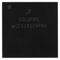
MCF5282CVF80 Freescale Semiconductor, MCF5282CVF80 Datasheet - Page 388

MCF5282CVF80
Manufacturer Part Number
MCF5282CVF80
Description
IC MPU 32BIT 66MHZ 256-MAPBGA
Manufacturer
Freescale Semiconductor
Series
MCF528xr
Datasheet
1.MCF5216CVM66J.pdf
(766 pages)
Specifications of MCF5282CVF80
Core Processor
Coldfire V2
Core Size
32-Bit
Speed
80MHz
Connectivity
CAN, EBI/EMI, Ethernet, I²C, SPI, UART/USART
Peripherals
DMA, LVD, POR, PWM, WDT
Number Of I /o
142
Program Memory Size
512KB (512K x 8)
Program Memory Type
FLASH
Ram Size
64K x 8
Voltage - Supply (vcc/vdd)
2.7 V ~ 3.6 V
Data Converters
A/D 8x10b
Oscillator Type
External
Operating Temperature
-40°C ~ 85°C
Package / Case
256-MAPBGA
Controller Family/series
ColdFire
Ram Memory Size
64KB
Embedded Interface Type
CAN, I2C, SPI, UART
No. Of Pwm Channels
8
Digital Ic Case Style
MAPBGA
Rohs Compliant
No
Package
256MA-BGA
Device Core
ColdFire
Family Name
MCF528x
Maximum Speed
80 MHz
Operating Supply Voltage
3.3 V
Data Bus Width
32 Bit
Number Of Programmable I/os
150
Interface Type
CAN/Ethernet/I2C/QSPI/UART
On-chip Adc
8-chx10-bit
Number Of Timers
12
Lead Free Status / RoHS Status
Contains lead / RoHS non-compliant
Eeprom Size
-
Available stocks
Company
Part Number
Manufacturer
Quantity
Price
Company:
Part Number:
MCF5282CVF80
Manufacturer:
FREESCALE
Quantity:
12 388
Company:
Part Number:
MCF5282CVF80
Manufacturer:
Freescale Semiconductor
Quantity:
10 000
Company:
Part Number:
MCF5282CVF80J
Manufacturer:
Freescale Semiconductor
Quantity:
10 000
- Current page: 388 of 766
- Download datasheet (9Mb)
GPTE
General Purpose Timer Modules (GPTA and GPTB)
The PORTTn data direction register controls the data direction of an input capture pin. External pin
conditions trigger input captures on input capture pins configured as inputs.
To configure a pin for input capture:
PORTTnDDR does not affect the data direction of an output compare pin. The output compare function
overrides the data direction register but does not affect the state of the data direction register.
To configure a pin for output compare:
Table 20-23
20-20
N
0
0
1
1
1
1
1
1
1
1
1
1
1. Clear the pin’s IOS bit in GPTIOS.
2. Clear the pin’s DDR bit in PORTTnDDR.
3. Write to GPTCTL2 to select the input edge to detect.
1. Set the pin’s IOS bit in GPTIOS.
2. Write the output compare value to GPTCn.
3. Clear the pin’s DDR bit in PORTTnDDR.
4. Write to the OMn/OLn bits in GPTCTL1 to select the output action.
DDR
0
1
0
1
0
1
0
1
0
1
0
1
1
shows how various timer settings affect pin functionality.
GPTIOS
1 (OC)
0 (IC)
X
X
0
0
0
0
0
1
1
1
4
disable
EDGx
[B:A]
0 (IC
<> 0
<> 0
<> 0
<> 0
X
d)
X
X
X
X
X
0
(3)
MCF5282 and MCF5216 ColdFire Microcontroller User’s Manual, Rev. 3
OMx/
OLx
<> 0
<> 0
Table 20-23. GPT Settings and Pin Functions
0
X
X
X
X
X
X
X
X
0
5
2
OC3Mx
X
X
0
0
0
0
1
1
0
0
0
0
3
Data
Out
Out
Out
Out
Out
Out
Out
Pin
Dir.
In
In
In
In
In
OC action Output compare Pin readable only if DDR = 0
OC action Output compare Pin driven by OC action
Data reg.
Data reg.
Data reg.
Data reg.
Data reg.
Driven
Ext.
Ext.
Ext.
Ext.
Ext.
Pin
by
Digital output
Digital output
Digital output
Digital output
Digital output
Digital input
Digital input
Digital input
digital input
digital input
Function
IC and
IC and
Pin
GPT disabled by GPTEN = 0
GPT disabled by GPTEN = 0
Input capture disabled by EDGn
setting
Input capture disabled by EDGn
setting
Normal settings for input capture
Input capture of data driven to output
pin by CPU
OC3M setting has no effect because
IOS = 0
OC3M setting has no effect because
IOS = 0; input capture of data driven
to output pin by CPU
Output compare takes place but
does not affect the pin because of
the OMn/OLn setting
Output compare takes place but
does not affect the pin because of
the OMn/OLn setting
Freescale Semiconductor
Comments
(5)
(5)
Related parts for MCF5282CVF80
Image
Part Number
Description
Manufacturer
Datasheet
Request
R
Part Number:
Description:
Mcf5282 And Mcf5216 Coldfire Microcontroller User�s Manual
Manufacturer:
Freescale Semiconductor, Inc
Datasheet:
Part Number:
Description:
Manufacturer:
Freescale Semiconductor, Inc
Datasheet:
Part Number:
Description:
Manufacturer:
Freescale Semiconductor, Inc
Datasheet:
Part Number:
Description:
Manufacturer:
Freescale Semiconductor, Inc
Datasheet:
Part Number:
Description:
Manufacturer:
Freescale Semiconductor, Inc
Datasheet:
Part Number:
Description:
Manufacturer:
Freescale Semiconductor, Inc
Datasheet:
Part Number:
Description:
Manufacturer:
Freescale Semiconductor, Inc
Datasheet:
Part Number:
Description:
Manufacturer:
Freescale Semiconductor, Inc
Datasheet:
Part Number:
Description:
Manufacturer:
Freescale Semiconductor, Inc
Datasheet:
Part Number:
Description:
Manufacturer:
Freescale Semiconductor, Inc
Datasheet:
Part Number:
Description:
Manufacturer:
Freescale Semiconductor, Inc
Datasheet:
Part Number:
Description:
Manufacturer:
Freescale Semiconductor, Inc
Datasheet:
Part Number:
Description:
Manufacturer:
Freescale Semiconductor, Inc
Datasheet:
Part Number:
Description:
Manufacturer:
Freescale Semiconductor, Inc
Datasheet:
Part Number:
Description:
Manufacturer:
Freescale Semiconductor, Inc
Datasheet:


