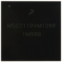
KMSC7119VM1200 Freescale Semiconductor, KMSC7119VM1200 Datasheet - Page 20

KMSC7119VM1200
Manufacturer Part Number
KMSC7119VM1200
Description
DSP 16BIT W/DDR CTRLR 400-MAPBGA
Manufacturer
Freescale Semiconductor
Series
MSC711x StarCorer
Type
Fixed Pointr
Datasheet
1.MSC7119VF1200.pdf
(60 pages)
Specifications of KMSC7119VM1200
Interface
Host Interface, I²C, UART
Clock Rate
300MHz
Non-volatile Memory
ROM (8 kB)
On-chip Ram
464kB
Voltage - I/o
3.30V
Voltage - Core
1.20V
Operating Temperature
-40°C ~ 105°C
Mounting Type
*
Package / Case
400-MAPBGA
Lead Free Status / RoHS Status
Lead free / RoHS Compliant
Available stocks
Company
Part Number
Manufacturer
Quantity
Price
Company:
Part Number:
KMSC7119VM1200
Manufacturer:
Freescale Semiconductor
Quantity:
10 000
Electrical Characteristics
Table 6 lists the DDR DRAM capacitance.
20
Tri-state (high impedance off state) leakage current,
V
Signal low input current, V
Signal high input current, V
Output high voltage, I
Output low voltage, I
Typical power at 300 MHz
Notes:
Input/output capacitance: DQ, DQS
Delta input/output capacitance: DQ, DQS
Note:
IN
= V
DDIO
1.
2.
3.
4.
5.
These values were measured under the following conditions:
• V
• f = 1 MHz
• T
• V
• V
A
DDM
OUT
OUT
= 25°C
The value of V
V
exceed ±2% of the DC value.
V
to V
Output leakage for the memory interface is measured with all outputs disabled, 0 V ≤ V
The core power values were measured.using a standard EFR pattern at typical conditions (25°C, 300 MHz, 1.2 V core).
REF
TT
= V
(peak to peak) = 0.2 V
= 2.5 V ± 0.125 V
REF
is not applied directly to the MSC7119 device. It is the level measured at the far end signal termination. It should be equal
OL
Characteristic
must be equal to 50% of V
DDM
OH
. This rail should track variations in the DC level of V
= 5 mA
= –2 mA, except open drain pins
/2
5
IL
IH
= 0.4 V
= 2.0 V
DDM
Parameter/Condition
at the MSC7119 device must remain within 50 mV of V
Table 5. DC Electrical Characteristics (continued)
DDM
Table 6. DDR DRAM Capacitance
and track V
MSC7119 Data Sheet, Rev. 8
Symbol
DDM
V
V
I
I
OZ
I
P
OH
H
OL
L
variations as measured at the receiver. Peak-to-peak noise must not
REF
.
Min
–1.0
–1.0
–1.0
2.0
—
—
DDM
at the DRAM device at all times.
Symbol
Typical
324.0
C
0.09
0.09
0.09
C
3.0
OUT
DIO
0
IO
≤ V
DDM
Freescale Semiconductor
.
Max
30
30
Max
0.4
—
—
1
1
1
Unit
pF
pF
Unit
mW
µA
µA
µA
V
V


