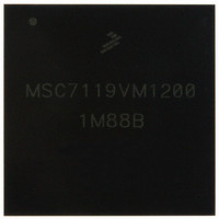
KMSC7119VM1200 Freescale Semiconductor, KMSC7119VM1200 Datasheet - Page 52

KMSC7119VM1200
Manufacturer Part Number
KMSC7119VM1200
Description
DSP 16BIT W/DDR CTRLR 400-MAPBGA
Manufacturer
Freescale Semiconductor
Series
MSC711x StarCorer
Type
Fixed Pointr
Datasheet
1.MSC7119VF1200.pdf
(60 pages)
Specifications of KMSC7119VM1200
Interface
Host Interface, I²C, UART
Clock Rate
300MHz
Non-volatile Memory
ROM (8 kB)
On-chip Ram
464kB
Voltage - I/o
3.30V
Voltage - Core
1.20V
Operating Temperature
-40°C ~ 105°C
Mounting Type
*
Package / Case
400-MAPBGA
Lead Free Status / RoHS Status
Lead free / RoHS Compliant
Available stocks
Company
Part Number
Manufacturer
Quantity
Price
Company:
Part Number:
KMSC7119VM1200
Manufacturer:
Freescale Semiconductor
Quantity:
10 000
Hardware Design Considerations
3.4.3
After a power-on reset, the PLL is bypassed and the device is directly clocked from the
slowly during the boot process. After the boot program is loaded, it can enable the PLL and start the device operating at a higher
speed. The MSC7119 can boot from an external host through the HDI16 or download a user program through the I
boot operating mode is set by configuring the
See the MSC711x Reference Manual for details of boot program operation.
3.4.3.1
If the MSC7119 device boots from an external host through the HDI16, the port is configured as follows:
52
HDI Boot Modes
SPI Boot Modes - Using HA3, HCS2, BM3, BM2 Pins
SPI Boot Modes - Using URXD, UTXD, SCL, SDA Pins
I
Reserved
Notes:
BM[3–0]
2
C Boot Modes
0000
0101
0010
0111
0100
1000
1001
1010
1011
1100
0001
0011
0110
1101
1110
1111
•
•
•
•
Operate in Non-DMA mode.
Operate in polled mode on the device side.
Operate in polled mode on the external host side.
External host must write four 16-bit values at a time with the first word as the most significant and the fourth word as
the least significant.
1.
2.
3.
SPI (SW)
SPI (SW)
Reserved
Reserved
Reserved
Reserved
Reserved
SPI (SW)
SPI (SW)
SPI (SW)
The clock divider determines the value used in the clock module CLKCTRL[PLLDVF] field.
The clock multiplier determines the value used in the clock module CLKCTRL[PLLMLTF] field.
F
Boot
HDI16
HDI16
HDI16
HDI16
HDI16
Boot
max
Port
HDI16 Boot
I
2
C
is determined by the maximum frequency of the peripheral and of the SC1400 core as specified in the data sheet.
Input Clock
22.2-25 MHz
25-33.3 MHz
44.3-50 MHz
15.6-25 MHz
44.3-75 MHz
Frequency
33-66 MHz
33-50 MHz
< 100 MHz
< F
< F
< F
—
—
—
—
—
max
max
max
Table 35. Boot Mode Source Selection
Divide
Clock
N/A
N/A
N/A
N/A
—
—
—
—
—
1
2
3
2
1
2
3
BM[0–3]
MSC7119 Data Sheet, Rev. 8
PLL
N/A
N/A
N/A
N/A
12
32
12
12
17
16
18
—
—
—
—
—
signals sampled at the rising edge of
CKSEL
00
11
01
11
11
00
11
11
11
00
00
—
—
—
—
—
RNG
Bit
—
—
—
—
—
0
1
1
1
1
0
0
0
0
0
0
133–212.5 MHz
266–300 MHz
200–266 MHz
132–264 MHz
266–300 MHz
132–200 MHz
133–225 MHz
Core Clock
Frequency
< 100 MHz
< F
< F
< F
—
—
—
—
—
max
max
max
CLKIN
PORESET,
pin. Thus, the device operates
Not clocked by the PLL.
Can boot as 8- or 16-bit HDI.
Can boot as 8- or 16-bit HDI.
The boot program automatically
determines whether EEPROM
or Flash memory.
Boots through different set of
pins.
Not clocked by the PLL.
I
rate of 400 Kbps. With a clock
divider of 128, this limits the
maximum input clock frequency
to 100 MHz.
2
C is limited to a maximum bit
Freescale Semiconductor
as shown in Table 35.
Comments
—
—
—
—
—
2
C port. The


