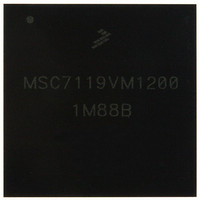
KMSC7119VM1200 Freescale Semiconductor, KMSC7119VM1200 Datasheet - Page 42

KMSC7119VM1200
Manufacturer Part Number
KMSC7119VM1200
Description
DSP 16BIT W/DDR CTRLR 400-MAPBGA
Manufacturer
Freescale Semiconductor
Series
MSC711x StarCorer
Type
Fixed Pointr
Datasheet
1.MSC7119VF1200.pdf
(60 pages)
Specifications of KMSC7119VM1200
Interface
Host Interface, I²C, UART
Clock Rate
300MHz
Non-volatile Memory
ROM (8 kB)
On-chip Ram
464kB
Voltage - I/o
3.30V
Voltage - Core
1.20V
Operating Temperature
-40°C ~ 105°C
Mounting Type
*
Package / Case
400-MAPBGA
Lead Free Status / RoHS Status
Lead free / RoHS Compliant
Available stocks
Company
Part Number
Manufacturer
Quantity
Price
Company:
Part Number:
KMSC7119VM1200
Manufacturer:
Freescale Semiconductor
Quantity:
10 000
Hardware Design Considerations
3.2
This section outlines the MSC7119 power considerations: power supply, power sequencing, power planes, decoupling, power
supply filtering, and power consumption. It also presents a recommended power supply design and options for low-power
consumption. For information on AC/DC electrical specifications and thermal characteristics, refer to Section 2.
3.2.1
The MSC7119 requires four input voltages, as shown in Table 32.
You should supply the MSC7119 core voltage via a variable switching supply or regulator to allow for compatibility with
possible core voltage changes on future silicon revisions. The core voltage is supplied with 1.2 V (+5% and –10%) across V
and
the DDR memory controller block. The memory voltage is supplied with 2.5 V across V
is supplied across V
(Stub Series Terminated Logic for 2.5 Volts (STTL_2)) for memory voltage supply requirements.
3.2.2
One consequence of multiple power supplies is that the voltage rails ramp up at different rates when power is initially applied.
The rates depend on the power supply, the type of load on each power supply, and the way different voltages are derived. It is
extremely important to observe the power up and power down sequences at the board level to avoid latch-up, forward biasing
of ESD devices, and excessive currents, which all lead to severe device damage.
Note:
42
GND
There are five possible power-up/power-down sequence cases. The first four cases listed in the following sections are
recommended for new designs. The fifth case is not recommended for new designs and must be carefully evaluated
for current spike risks based on actual information for the specific application.
and the I/O section is supplied with 3.3 V (± 10%) across V
Core
Memory
Reference
I/O
Power Supply Design Considerations
Power Supply
Power Sequencing
REF
Voltage
and
GND
and must be between 0.49 × V
MSC7119 Data Sheet, Rev. 8
Table 32. MSC7119 Voltages
Symbol
V
V
V
V
DDM
DDIO
DDM
DDC
REF
DDIO
and 0.51 × V
and
GND.
DDM
The memory and reference voltages supply
. Refer to the JEDEC standard JESD8
DDM
and
GND
Freescale Semiconductor
. The reference voltage
Value
1.25 V
1.2 V
2.5 V
3.3 V
DDC


