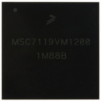
KMSC7119VM1200 Freescale Semiconductor, KMSC7119VM1200 Datasheet - Page 48

KMSC7119VM1200
Manufacturer Part Number
KMSC7119VM1200
Description
DSP 16BIT W/DDR CTRLR 400-MAPBGA
Manufacturer
Freescale Semiconductor
Series
MSC711x StarCorer
Type
Fixed Pointr
Datasheet
1.MSC7119VF1200.pdf
(60 pages)
Specifications of KMSC7119VM1200
Interface
Host Interface, I²C, UART
Clock Rate
300MHz
Non-volatile Memory
ROM (8 kB)
On-chip Ram
464kB
Voltage - I/o
3.30V
Voltage - Core
1.20V
Operating Temperature
-40°C ~ 105°C
Mounting Type
*
Package / Case
400-MAPBGA
Lead Free Status / RoHS Status
Lead free / RoHS Compliant
Available stocks
Company
Part Number
Manufacturer
Quantity
Price
Company:
Part Number:
KMSC7119VM1200
Manufacturer:
Freescale Semiconductor
Quantity:
10 000
Hardware Design Considerations
3.2.3
Each power supply pin (
should be provided with a low-impedance path to ground. The power supply pins drive distinct groups of logic on the device.
The MSC7119
associated printed circuit traces connecting to device power pins and
lead. A minimum four-layer board that employs two inner layers as power and
for DDR Controller power guidelines.
3.2.4
Both the I/O voltage and core voltage should be decoupled for switching noise. For I/O decoupling, use standard capacitor
values of 0.01 μF for every two to three voltage pins. For core voltage decoupling, use two levels of decoupling. The first level
should consist of a 0.01 µF high frequency capacitor with low effective series resistance (ESR) and effective series inductance
(ESL) for every two to three voltage pins. The second decoupling level should consist of two bulk/tantalum decoupling
capacitors, one 10 μF and one 47 μF, (with low ESR and ESL) mounted as closely as possible to the MSC7119 voltage pins.
Additionally, the maximum drop between the power supply and the DSP device should be 15 mV at 1 A.
3.2.5
The MSC7119
power supplied to this pin should be filtered with capacitors that have low and high frequency filtering characteristics.
can be connected to V
shown in Figure 35 is recommended. The PLL loop filter should be placed as closely as possible to the
located on the outside edge of the silicon package) to minimize noise coupled from nearby circuits.The 0.01 µF capacitor should
be closest to
should be kept short.
3.2.6
You can reduce power consumption in your design by controlling the power consumption of the following regions of the device:
For details, see the “Clocks and Power Management” chapter of the MSC711x Reference Manual.
48
•
•
•
•
Extended core. Use the SC1400 Stop and Wait modes by issuing a stop or wait instruction.
Clock synthesis module. Disable the PLL, timer, watchdog, or DDR clocks or disable the
AHB subsystem. Freeze or shut down the AHB subsystem using the GPSCTL[XBR_HRQ] bit.
Peripheral subsystem. Halt the individual on-device peripherals such as the DDR memory controller, Ethernet MAC,
HDI16, TDM, UART, I
V
Power Planes
Decoupling
PLL Power Supply Filtering
DDPLL
Power Consumption
V
V
DDC
DDPLL
, followed by the 0.1 µF capacitor, the 10 µF capacitor, and finally the 2-Ω resistor to
power supply pins should be bypassed to ground using decoupling capacitors. The capacitor leads and
DDC
power signal provides power to the clock generation PLL. To ensure stability of the internal clock, the
V
DDC
through a 2 Ω resistor. V
,
V
DDM,
2
C, and timer modules.
V
DDC
and
Figure 35. PLL Power Supply Filter Circuits
V
DDIO
2
Ω
) should have a low-impedance path to the board power supply. Each
MSC7119 Data Sheet, Rev. 8
SSPLL
10 µF
can be tied directly to the
GND
0.1 µF 0.01 µF
should be kept to less than half an inch per capacitor
GND
GND
V
planes is recommended. See Section 3.5
DDPLL
plane. A circuit similar to the one
CLKO
Freescale Semiconductor
V
DDPLL
pin.
V
DDC
pin (which are
. These traces
GND
V
DDPLL
pin


