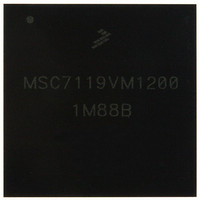
KMSC7119VM1200 Freescale Semiconductor, KMSC7119VM1200 Datasheet - Page 22

KMSC7119VM1200
Manufacturer Part Number
KMSC7119VM1200
Description
DSP 16BIT W/DDR CTRLR 400-MAPBGA
Manufacturer
Freescale Semiconductor
Series
MSC711x StarCorer
Type
Fixed Pointr
Datasheet
1.MSC7119VF1200.pdf
(60 pages)
Specifications of KMSC7119VM1200
Interface
Host Interface, I²C, UART
Clock Rate
300MHz
Non-volatile Memory
ROM (8 kB)
On-chip Ram
464kB
Voltage - I/o
3.30V
Voltage - Core
1.20V
Operating Temperature
-40°C ~ 105°C
Mounting Type
*
Package / Case
400-MAPBGA
Lead Free Status / RoHS Status
Lead free / RoHS Compliant
Available stocks
Company
Part Number
Manufacturer
Quantity
Price
Company:
Part Number:
KMSC7119VM1200
Manufacturer:
Freescale Semiconductor
Quantity:
10 000
Electrical Characteristics
2.5.2
This section describes important requirements for configuring clock frequencies in the MSC7119 device when using the PLL
block. To configure the device clocking, you must program four fields in the Clock Control Register (CLKCTL):
There are restrictions on the frequency range permitted at the beginning of the multiplication portion of the PLL that affect the
allowable values for the PLLDVF and PLLMLTF fields. The following sections define these restrictions and provide guidelines
to configure the device clocking when using the PLL. Refer to the Clock and Power Management chapter in the MSC711x
Reference Manual for details on the clock programming model.
2.5.2.1
There are two restrictions for correct usage of the PLL block:
When programming the PLL for a desired output frequency using the PLLDVF, PLLMLTF, and RNG fields, you must meet
these constraints.
2.5.2.2
The value of the PLLDVF field determines the allowable
22
Note:
Field Value
PLLDVF
•
•
•
•
•
•
0x00
0x01
0x02
0x03
0x04
0x05
0x06
0x07
0x08
0x09
PLLDVF field. Specifies the PLL division factor (PLLDVF + 1) to divide the input clock frequency
of the divider block is the input to the multiplier block.
PLLMLTF field. Specifies the PLL multiplication factor (PLLMLTF + 1). The output from the multiplier block is the
loop frequency F
RNG field. Selects the available PLL frequency range for F
when the RNG bit is cleared (0).
CKSEL field. Selects F
The input frequency to the PLL multiplier block (that is, the output of the divider) must be in the range 10–25 MHz.
The output frequency of the PLL multiplier must be in the range 266–532 MHz.
The maximum CLKIN frequency is 100 MHz. Therefore, the PLLDVF value must be in the range from 1–10.
Configuring Clock Frequencies
PLL Multiplier Restrictions
Input Division Factors and Corresponding CLKIN Frequency Range
Input Divide
Factor
10
1
2
3
4
5
6
7
8
9
LOOP
Table 9. CLKIN Frequency Ranges by Divide Factor Value
.
CLKIN
CLKIN Frequency Range
, F
VCO
40 to 100 MHz
50 to 100 MHz
60 to 100 MHz
70 to 100 MHz
80 to 100 MHz
90 to 100 MHz
10 to 25 MHz
20 to 50 MHz
30 to 75 MHz
, or F
100 MHz
MSC7119 Data Sheet, Rev. 8
VCO
/2 as the source for the core clock.
CLKIN
frequency range, as shown in Table 9.
Input Division by 1
Input Division by 2
Input Division by 3
Input Division by 4
Input Division by 5
Input Division by 6
Input Division by 7
Input Division by 8
Input Division by 9
Input Division by 10
VCO
, either F
LOOP
when the RNG bit is set (1) or F
Comments
Freescale Semiconductor
F
CLKIN
. The output
LOOP
/2


