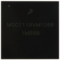
KMSC7119VM1200 Freescale Semiconductor, KMSC7119VM1200 Datasheet - Page 56

KMSC7119VM1200
Manufacturer Part Number
KMSC7119VM1200
Description
DSP 16BIT W/DDR CTRLR 400-MAPBGA
Manufacturer
Freescale Semiconductor
Series
MSC711x StarCorer
Type
Fixed Pointr
Datasheet
1.MSC7119VF1200.pdf
(60 pages)
Specifications of KMSC7119VM1200
Interface
Host Interface, I²C, UART
Clock Rate
300MHz
Non-volatile Memory
ROM (8 kB)
On-chip Ram
464kB
Voltage - I/o
3.30V
Voltage - Core
1.20V
Operating Temperature
-40°C ~ 105°C
Mounting Type
*
Package / Case
400-MAPBGA
Lead Free Status / RoHS Status
Lead free / RoHS Compliant
Available stocks
Company
Part Number
Manufacturer
Quantity
Price
Company:
Part Number:
KMSC7119VM1200
Manufacturer:
Freescale Semiconductor
Quantity:
10 000
Hardware Design Considerations
3.5.3
The general routing considerations for the DDR are as follows:
3.5.4
The DDR clock distribution considerations are as follows:
3.5.5
The DDR data routing considerations are as follows:
56
•
•
•
•
•
•
•
•
•
•
•
•
•
•
•
•
•
•
All DDR signals must be routed next to a solid reference:
— For data, next to solid ground planes.
— For address/command, power planes if necessary.
All DDR signals must be impedance controlled. This is system dependent, but typical values are 50–60 ohm.
Minimize other cross-talk opportunities. As possible, maintain at least a four times the trace width spacing between all
DDR signals to non-DDR signals.
Keep the number of vias to a minimum to eliminate additional stubs and capacitance.
Signal group routing priorities are as follows:
— DDR clocks.
— Route MVTT/MVREF.
— Data group.
— Command/address.
Minimize data bit jitter by trace matching.
DDR controller supports six clock pairs:
— 2 DIMM modules.
— Up to 36 discrete chips.
For route traces as for any other differential signals:
— Maintain proper difference pair spacing.
— Match pair traces within 25 mm.
Match all clock traces to within 100 mm.
Keep all clocks equally loaded in the system.
Route clocks on inner critical layers.
Route each data group (8-bits data +
Take care to match trace lengths, which is extremely important.
To make trace matching easier, let adjacent groups be routed on alternate critical layers.
Pin swap bits within a byte group to facilitate routing (discrete case).
Tight trace matching is recommended within the DDR data group. Keep each 8-bit datum and its DM signal within ±
25 mm of its respective strobe.
Minimize lengths across the entire DDR channel:
— Between all groups maintain a delta of no more than 500 mm.
— Allows greater flexibility in the design for readjustments as needed.
DDR data group separation:
— If stack-up allows, keep DDR data groups away from the address and control nets.
— Route address and control on separate critical layers.
— If resistor networks (RNs) are used, attempt to keep data and command lines in separate packages.
General Routing
Routing Clock Distribution
Data Routing
DQS
MSC7119 Data Sheet, Rev. 8
+
DM
) on the same layer. Avoid switching layers within a byte group.
Freescale Semiconductor


