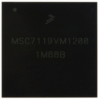
KMSC7119VM1200 Freescale Semiconductor, KMSC7119VM1200 Datasheet - Page 27

KMSC7119VM1200
Manufacturer Part Number
KMSC7119VM1200
Description
DSP 16BIT W/DDR CTRLR 400-MAPBGA
Manufacturer
Freescale Semiconductor
Series
MSC711x StarCorer
Type
Fixed Pointr
Datasheet
1.MSC7119VF1200.pdf
(60 pages)
Specifications of KMSC7119VM1200
Interface
Host Interface, I²C, UART
Clock Rate
300MHz
Non-volatile Memory
ROM (8 kB)
On-chip Ram
464kB
Voltage - I/o
3.30V
Voltage - Core
1.20V
Operating Temperature
-40°C ~ 105°C
Mounting Type
*
Package / Case
400-MAPBGA
Lead Free Status / RoHS Status
Lead free / RoHS Compliant
Available stocks
Company
Part Number
Manufacturer
Quantity
Price
Company:
Part Number:
KMSC7119VM1200
Manufacturer:
Freescale Semiconductor
Quantity:
10 000
Figure 6 shows the DDR DRAM output timing diagram.
Freescale Semiconductor
Notes:
No.
209
210
211
212
Dn/DQMn output setup with respect to DQSn
Dn/DQMn output hold with respect to DQSn
DQSn preamble start
DQSn epilogue end
1.
2.
3.
4.
5.
DQMn
DQSn
All CK/CK referenced measurements are made from the crossing of the two signals ±0.1 V.
t
arrives 75–125% of a DRAM cycle after the write command is issued. Any skew between DQSn and CK must be considered
when trying to achieve this 75%–125% goal. The TCFG2[WRDD] bits can be used to shift DQSn by 1/4 DRAM cycle
increments. The skew in this case refers to an internal skew existing at the signal connections. By default, the CK/CK crossing
occurs in the middle of the control signal (An/RAS/CAS/WE/CKE) tenure. Setting TCFG2[ACSM] bit shifts the control signal
assertion 1/2 DRAM cycle earlier than the default timing. This means that the signal is asserted no earlier than 600 ps before
the CK/CK crossing and no later than 600 ps after the crossing time; the device uses 1200 ps of the skew budget (the interval
from –600 to +600 ps). Timing is verified by referencing the falling edge of CK. See Chapter 10 of the MSC711x Reference
Manual for details.
Determined by maximum possible skew between a data strobe (DQS) and any corresponding bit of data. The data strobe
should be centered inside of the data eye.
Please note that this spec is in reference to the DQSn first rising edge. It could also be referenced from CK(r), but due to
programmable delay of the write strobes (TCFG2[WRDD]), there pre-amble may be extended for a full DRAM cycle. For this
reason, we reference from DQSn.
All outputs are referenced to the rising edge of CK. Note that this is essentially the CK/DQSn skew in spec 208. In addition
there is no real “maximum” time for the epilogue end. JEDEC does not require this is as a device limitation, but simply for the
chip to guarantee fast enough write-to-read turn-around times. This is already guaranteed by the memory controller operation.
RAS
CAS
CKE
DDKHMH
WE
CK
CK
An
Dn
can be modified through the TCFG2[WRDD] DQSS override bits. The DRAM requires that the first write data strobe
5
4
Parameter
204
206
Table 18. DDR DRAM Output AC Timing (continued)
Write A0
Figure 6. DDR DRAM Output Timing Diagram
207
205
209
200
210
211
MSC7119 Data Sheet, Rev. 8
3
NOOP
3
D0
D1
208
209
Symbol
t
t
t
t
t
t
DDKHDS,
DDKHDX,
DDKHMP
DDKHME
DDKLDS
DDKLDX
210
0.25 × t
0.25 × t
–0.25 × t
–600
Min
CK
CK
– 750
– 750
CK
212
Electrical Characteristics
Max
600
—
—
—
Unit
ps
ps
ps
ps
27


