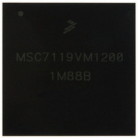
KMSC7119VM1200 Freescale Semiconductor, KMSC7119VM1200 Datasheet - Page 32

KMSC7119VM1200
Manufacturer Part Number
KMSC7119VM1200
Description
DSP 16BIT W/DDR CTRLR 400-MAPBGA
Manufacturer
Freescale Semiconductor
Series
MSC711x StarCorer
Type
Fixed Pointr
Datasheet
1.MSC7119VF1200.pdf
(60 pages)
Specifications of KMSC7119VM1200
Interface
Host Interface, I²C, UART
Clock Rate
300MHz
Non-volatile Memory
ROM (8 kB)
On-chip Ram
464kB
Voltage - I/o
3.30V
Voltage - Core
1.20V
Operating Temperature
-40°C ~ 105°C
Mounting Type
*
Package / Case
400-MAPBGA
Lead Free Status / RoHS Status
Lead free / RoHS Compliant
Available stocks
Company
Part Number
Manufacturer
Quantity
Price
Company:
Part Number:
KMSC7119VM1200
Manufacturer:
Freescale Semiconductor
Quantity:
10 000
Electrical Characteristics
2.5.7
32
Notes:
No.
44a
44b
44c
40
45
46
47
48
49
50
51
52
53
54
55
56
57
58
61
62
63
64
Host Interface Clock period
Read data strobe minimum assertion width
HACK read minimum assertion width
Read data strobe minimum deassertion width
HACK read minimum deassertion width
Read data strobe minimum deassertion width
reads
HACK minimum deassertion width after “Last Data Register” reads
Write data strobe minimum assertion width
HACK write minimum assertion width
Write data strobe minimum deassertion width
HACK write minimum deassertion width after ICR, CVR and Data Register
writes
Host data input minimum setup time before write data strobe deassertion
Host data input minimum setup time before HACK write deassertion
Host data input minimum hold time after write data strobe deassertion
Host data input minimum hold time after HACK write deassertion
Read data strobe minimum assertion to output data active from high
impedance
HACK read minimum assertion to output data active from high impedance
Read data strobe maximum assertion to output data valid
HACK read maximum assertion to output data valid
Read data strobe maximum deassertion to output data high impedance
HACK read maximum deassertion to output data high impedance
Output data minimum hold time after read data strobe deassertion
Output data minimum hold time after HACK read deassertion
HCS[1–2] minimum assertion to read data strobe assertion
HCS[1–2] minimum assertion to write data strobe assertion
HCS[1–2] maximum assertion to output data valid
HCS[1–2] minimum hold time after data strobe deassertion
HA[0–2], HRW minimum setup time before data strobe assertion
HA[0–2], HRW minimum hold time after data strobe deassertion
Maximum delay from read data strobe deassertion to host request
deassertion for “Last Data Register” read
Maximum delay from write data strobe deassertion to host request
deassertion for “Last Data Register” write
Minimum delay from DMA HACK (OAD=0) or Read/Write data
strobe(OAD=1) deassertion to HREQ assertion.
Maximum delay from DMA HACK (OAD=0) or Read/Write data
strobe(OAD=1) assertion to HREQ deassertion
1.
2.
3.
4.
5.
6.
7.
8.
9.
10. The host request is HREQ/HREQ in the single host request mode and HRRQ/HRRQ and HTRQ/HTRQ in the double host
11. Compute the value using the expression.
12. The read and write data strobe minimum deassertion width for non-”last data register” accesses in single and dual data strobe
T
In the timing diagrams below, the controls pins are drawn as active low. The pin polarity is programmable.
V
The read data strobe is HRD/HRD in the dual data strobe mode and HDS/HDS in the single data strobe mode.
For 64-bit transfers, the “last data register” is the register at address 0x7, which is the last location to be read or written in data
transfers. This is RX0/TX0 in the little endian mode (HBE = 0), or RX3/TX3 in the big endian mode (HBE = 1).
This timing is applicable only if a read from the “last data register” is followed by a read from the RX[0–3] registers without first
polling RXDF or HREQ bits, or waiting for the assertion of the HREQ/HREQ signal.
This timing is applicable only if two consecutive reads from one of these registers are executed.
The write data strobe is HWR in the dual data strobe mode and HDS in the single data strobe mode.
The data strobe is host read (HRD/HRD) or host write (HWR/HWR) in the dual data strobe mode and host data strobe
(HDS/HDS) in the single data strobe mode.
request mode. HRRQ/HRRQ is deasserted only when HOTX fifo is empty, HTRQ/HTRQ is deasserted only if HORX fifo is full
modes is based on timings 57 and 58.
HDI16 Signals
5,6
5
CORE
DD
, or between two consecutive CVR, ICR, or ISR reads
= 3.3 V ± 0.15 V; T
4
= core clock period. At 300 MHz, T
Characteristics
J
= –40°C to +105 °C, C
Table 25. Host Interface (HDI16) Timing
4, 5, 10
5,8,10
8
4
MSC7119 Data Sheet, Rev. 8
8
4
4
3
after “Last Data Register”
CORE
L
= 3.333 ns.
= 30 pF for maximum delay timings and C
4
4
9
8
7
9
9
4
5,6
8
4
8
(2.0 × T
(2.0 × T
(3.0 × T
(3.0 × T
(2.0 × T
(5.0 × T
2.0 × T
Expression
1.5 × T
2.5 × T
1.5 × T
2.5 × T
1, 2
T
CORE
CORE
CORE
CORE
CORE
CORE
CORE
CORE
—
—
—
—
—
—
—
—
—
—
CORE
CORE
CORE
CORE
) + 8.0
) + 6.0
) + 1.0
) + 6.0
) + 6.0
) + 6.0
+ 9.0
L
= 0 pF for minimum delay timings.
Freescale Semiconductor
Note 11
Note 11
Note 11
Note 11
Note 11
Note 11
Note 11
Note 11
Note 11
Note 11
Note 11
Value
Note 1
2.5
2.5
1.0
9.0
1.0
0.5
0.0
0.5
5.0
5.0
Unit
ns
ns
ns
ns
ns
ns
ns
ns
ns
ns
ns
ns
ns
ns
ns
ns
ns
ns
ns
ns
ns
ns


