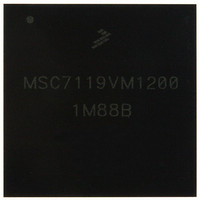
KMSC7119VM1200 Freescale Semiconductor, KMSC7119VM1200 Datasheet - Page 50

KMSC7119VM1200
Manufacturer Part Number
KMSC7119VM1200
Description
DSP 16BIT W/DDR CTRLR 400-MAPBGA
Manufacturer
Freescale Semiconductor
Series
MSC711x StarCorer
Type
Fixed Pointr
Datasheet
1.MSC7119VF1200.pdf
(60 pages)
Specifications of KMSC7119VM1200
Interface
Host Interface, I²C, UART
Clock Rate
300MHz
Non-volatile Memory
ROM (8 kB)
On-chip Ram
464kB
Voltage - I/o
3.30V
Voltage - Core
1.20V
Operating Temperature
-40°C ~ 105°C
Mounting Type
*
Package / Case
400-MAPBGA
Lead Free Status / RoHS Status
Lead free / RoHS Compliant
Available stocks
Company
Part Number
Manufacturer
Quantity
Price
Company:
Part Number:
KMSC7119VM1200
Manufacturer:
Freescale Semiconductor
Quantity:
10 000
Hardware Design Considerations
3.3.2
Peripherals include the DDR memory controller, Ethernet controller, DMA controller, HDI16, TDM, UART, timers, GPIOs,
and the I
following equation which assumes an effective load of 20 pF, core voltage swing of 1.2 V, and a switching frequency of 100
MHz. This yields:
Multiply this value by the number of peripherals used in the application to compute the total peripheral power consumption.
3.3.3
Estimation of power consumption by the DDR memory system is complex. It varies based on overall system signal line usage,
termination and load levels, and switching rates. Because the DDR memory includes terminations external to the MSC7119
device, the 2.5 V power source provides the power for the termination, which is a static value of 16 mA per signal driven high.
The dynamic power is computed, however, using a differential voltage swing of ±0.200 V, yielding a peak-to-peak swing of 0.4
V. The equations for computing the DDR power are:
As an example, assume the following:
In this example, the DDR memory power consumption is:
3.3.4
The estimation of the I/O power is similar to the computation of the peripheral power estimates. The power consumption per
signal line is computed assuming a maximum load of 20 pF, a voltage swing of 3.3 V, and a switching frequency of 25 MHz,
which yields:
Multiply this number by the number of I/O signal lines used in the application design to compute the total I/O power.
Note:
3.3.5
The leakage power is for all power supplies combined at a specific temperature. The value is temperature dependent. The
observed leakage value at room temperature is 64 mW.
50
pin activity value = (active data lines × % activity × % data switching) + (active address lines × % activity)
P
DDRIO
2
The signal loading depends on the board routing. For systems using a single DDR device, the load could be as low as
7 pF.
C module. Basic power consumption by each module is assumed to be the same and is computed by using the
= ((16 × 0.5) × 16 × 2.5) + (((16 × 0.6 × 0.5) + (3 × 0.6)) × 20 × (0.4)
Peripheral Power
External Memory Power
External I/O Power
Leakage Power
unused pins = 16 (DDR uses 16-pin mode)
% driven high = 50%
active data lines = 16
% activity = 60%
% data switching = 50%
active address lines = 3
P
PERIPHERAL
P
DYNAMIC
P
IO
P
= 20 pF × (3.3 V)
STATIC
= (pin activity value) × 20 pF × (0.4 V)
= 20 pF × (1.2 V)
= (unused pins × % driven high) × 16 mA × 2.5 V
P
DDRIO
MSC7119 Data Sheet, Rev. 8
2
× 25 MHz × 10
2
= P
× 150 MHz × 10
STATIC
+ P
–3
DYNAMIC
= 5.44 mW per I/O line
–3
2
= 4.32 mW per peripheral
× 300 MHz × 10
2
× 300 × 10
–3
mW
–3
) = 326.3 mW
Freescale Semiconductor
Eqn. 10
Eqn. 12
Eqn. 11
Eqn. 6
Eqn. 7
Eqn. 8
Eqn. 9


