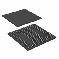
ADSP-BF538BBCZ-4F4 Analog Devices Inc, ADSP-BF538BBCZ-4F4 Datasheet - Page 14

ADSP-BF538BBCZ-4F4
Manufacturer Part Number
ADSP-BF538BBCZ-4F4
Description
IC, FLOAT-PT DSP, 16BIT, 400MHZ, BGA-316
Manufacturer
Analog Devices Inc
Series
Blackfinr
Type
Fixed Pointr
Datasheets
1.ADSP-BF538BBCZ-5F8.pdf
(56 pages)
2.ADSP-BF538BBCZ-4A.pdf
(56 pages)
3.ADSP-BF538BBCZ-4F4.pdf
(60 pages)
Specifications of ADSP-BF538BBCZ-4F4
No. Of Bits
16 Bit
Frequency
400MHz
Supply Voltage
1.2V
Embedded Interface Type
CAN, I2C, PPI, SPI, TWI, UART
No. Of I/o's
54
Flash Memory Size
512KB
Interface
CAN, SPI, SSP, TWI, UART
Clock Rate
400MHz
Non-volatile Memory
FLASH (512 kB)
On-chip Ram
148kB
Voltage - I/o
3.00V, 3.30V
Voltage - Core
1.20V
Operating Temperature
-40°C ~ 85°C
Mounting Type
Surface Mount
Package / Case
316-CSPBGA
Device Core Size
16b
Architecture
Modified Harvard
Format
Fixed Point
Clock Freq (max)
400MHz
Mips
400
Device Input Clock Speed
400MHz
Ram Size
32KB
Program Memory Size
512KB
Operating Supply Voltage (typ)
1.2/2.5/3.3V
Operating Supply Voltage (min)
0.8/2.25/2.7V
Operating Supply Voltage (max)
1.32/3.6V
Operating Temp Range
-40C to 85C
Operating Temperature Classification
Industrial
Mounting
Surface Mount
Pin Count
316
Package Type
CSPBGA
Lead Free Status / RoHS Status
Lead free / RoHS Compliant
For Use With
ADZS-BFAUDIO-EZEXT - BOARD EVAL AUDIO BLACKFIN
Lead Free Status / Rohs Status
Compliant
ADSP-BF538/ADSP-BF538F
internal logic except for the RTC logic. The 3.3 V V
domain supplies all the I/O except for the RTC crystal. There
are no sequencing requirements for the various power domains.
Table 6. Power Domains
The V
is to operate while the rest of the chip is powered down) or
should be connected to the V
V
nate state, and should also be powered even if the RTC
functionality is not being used in an application.
The power dissipated by a processor is largely a function of the
clock frequency of the processor and the square of the operating
voltage. For example, reducing the clock frequency by 25%
results in a 25% reduction in dynamic power dissipation, while
reducing the voltage by 25% reduces dynamic power dissipation
by more than 40%. Further, these power savings are additive, in
that if the clock frequency and supply voltage are both reduced,
the power savings can be dramatic.
The dynamic power management feature of the processor
allows both the processor’s input voltage (V
quency (f
The savings in power dissipation can be modeled using the
power savings factor and % power savings calculations.
The power savings factor is calculated as
where:
f
f
V
V
t
t
The power savings factor is calculated as
VOLTAGE REGULATION
The Blackfin processors provide an on-chip voltage regulator
that can generate appropriate V
V
tor tolerances and acceptable V
Power Domain
RTC Crystal I/O and Logic
All Internal Logic Except RTC
All I/O Except RTC
CCLKNOM
CCLKRED
NOM
RED
DDRTC
DDINTNOM
DDINTRED
DDEXT
is the duration running at f
% Power Savings
is the duration running at f
DDRTC
supply. See
should remain powered when the processor is in hiber-
is the reduced core clock frequency.
Power Savings Factor
is the nominal core clock frequency.
CCLK
=
is the reduced internal supply voltage.
is the nominal internal supply voltage.
should either be connected to a battery (if the RTC
---------------------- -
f
f
CCLKNOM
) to be dynamically controlled.
CCLKRED
Operating Conditions on Page 23
×
=
(
----------------------------
V
V
1 Power Savings Factor
DDINTNOM
DDINTRED
–
DDEXT
DDEXT
CCLKRED
DDINT
CCLKNOM
plane on the board. The
ranges for specific models.
voltage levels from the
2
.
×
.
----------- -
t
t
NOM
RED
DDINT
VDD Range
VDDRTC
VDDINT
V
DDEXT
) and clock fre-
)
DDEXT
×
Rev. D | Page 14 of 56 | July 2010
for regula-
100%
power
The regulator controls the internal logic voltage levels and is
programmable with the voltage regulator control register
(VR_CTL) in increments of 50 mV. To reduce standby power
consumption, the internal voltage regulator can be programmed
to remove power to the processor core while I/O power (V
V
is still being applied, eliminating the need for external buffers.
The voltage regulator can be activated from this power-down
state either through an RTC wake-up, a CAN wake-up, a
general-purpose wake-up, or by asserting RESET, all of which
will then initiate a boot sequence. The regulator can also be dis-
abled and bypassed at the user’s discretion.
Voltage Regulator Layout Guidelines
Regulator external component placement, board routing, and
bypass capacitors all have a significant effect on noise injected
into the other analog circuits on-chip. The VROUT1–0 traces
and voltage regulator external components should be consid-
ered as noise sources when doing board layout and should not
be routed or placed near sensitive circuits or components on the
board. All internal and I/O power supplies should be well
bypassed with bypass capacitors placed as close to the
ADSPBF538/ADSP-BF538F processors as possible.
For further details on the on-chip voltage regulator and related
board design guidelines, see the Switching Regulator Design
Considerations for ADSP-BF533 Blackfin Processor (EE-228)
applications note on the Analog Devices website
(www.analog.com)—use site search on “EE-228”.
CLOCK SIGNALS
The ADSP-BF538/ADSP-BF538F processors can be clocked by
an external crystal, a sine wave input, or a buffered, shaped
clock derived from an external clock oscillator.
(LOW-INDUCTANCE)
DDEXT
100μF
V
NOTE: DESIGNER SHOULD MINIMIZE
TRACE LENGTH TO FDS9431A.
) is still supplied. While in the hibernate state, I/O power
DDEXT
+
LOW ESR
10μF
100nF
Figure 6. Voltage Regulator Circuit
FDS9431A
SET OF DECOUPLING
CAPACITORS
ZHCS1000
INDUCTANCE WIRE
SHORT AND LOW-
10μH
100μF
100μF
+
+
DDRTC
V
V
GND
VR
VR
,
DDEXT
DDINT
OUT
OUT


