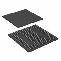
ADSP-BF538BBCZ-4F4 Analog Devices Inc, ADSP-BF538BBCZ-4F4 Datasheet - Page 44

ADSP-BF538BBCZ-4F4
Manufacturer Part Number
ADSP-BF538BBCZ-4F4
Description
IC, FLOAT-PT DSP, 16BIT, 400MHZ, BGA-316
Manufacturer
Analog Devices Inc
Series
Blackfinr
Type
Fixed Pointr
Datasheets
1.ADSP-BF538BBCZ-5F8.pdf
(56 pages)
2.ADSP-BF538BBCZ-4A.pdf
(56 pages)
3.ADSP-BF538BBCZ-4F4.pdf
(60 pages)
Specifications of ADSP-BF538BBCZ-4F4
No. Of Bits
16 Bit
Frequency
400MHz
Supply Voltage
1.2V
Embedded Interface Type
CAN, I2C, PPI, SPI, TWI, UART
No. Of I/o's
54
Flash Memory Size
512KB
Interface
CAN, SPI, SSP, TWI, UART
Clock Rate
400MHz
Non-volatile Memory
FLASH (512 kB)
On-chip Ram
148kB
Voltage - I/o
3.00V, 3.30V
Voltage - Core
1.20V
Operating Temperature
-40°C ~ 85°C
Mounting Type
Surface Mount
Package / Case
316-CSPBGA
Device Core Size
16b
Architecture
Modified Harvard
Format
Fixed Point
Clock Freq (max)
400MHz
Mips
400
Device Input Clock Speed
400MHz
Ram Size
32KB
Program Memory Size
512KB
Operating Supply Voltage (typ)
1.2/2.5/3.3V
Operating Supply Voltage (min)
0.8/2.25/2.7V
Operating Supply Voltage (max)
1.32/3.6V
Operating Temp Range
-40C to 85C
Operating Temperature Classification
Industrial
Mounting
Surface Mount
Pin Count
316
Package Type
CSPBGA
Lead Free Status / RoHS Status
Lead free / RoHS Compliant
For Use With
ADZS-BFAUDIO-EZEXT - BOARD EVAL AUDIO BLACKFIN
Lead Free Status / Rohs Status
Compliant
ADSP-BF538/ADSP-BF538F
General-Purpose Port Timing
Table 37
Table 37. General-Purpose Port Timing
Timer Cycle Timing
Table 38
input signal is asynchronous in “width capture mode” and
“external clock mode” and has an absolute maximum input fre-
quency of f
Table 38. Timer Cycle Timing
1
Parameter
Timing Requirement
t
Switching Characteristic
t
Parameter
Timing Characteristics
t
t
Switching Characteristic
t
The minimum pulse widths apply for TMRx input pins in width capture and external clock modes. They also apply to the PF1 or PPI_CLK input pins in PWM output mode.
WFI
GPOD
WL
WH
HTO
and
and
SCLK
Figure 29
Figure 30
/2 MHz.
TMRx OUTPUT
GPIO OUTPUT
TMRx INPUT
GP Port Pin Input Pulse Width
GP Port Pin Output Delay from CLKOUT Low
GPIO INPUT
Timer Pulse Width Input Low
Timer Pulse Width Input High
Timer Pulsewidth Output (measured in SCLK Cycles)
CLKOUT
CLKOUT
describe general-purpose operations.
describe timer expired operations. The
1
1
(Measured in SCLK Cycles)
(Measured in SCLK Cycles)
Figure 29. General-Purpose Port Cycle Timing
Figure 30. Timer PWM_OUT Cycle Timing
Rev. D | Page 44 of 56 | July 2010
t
TIS
t
WFI
t
WH
,t
t
WL
TIH
t
GPOD
t
TOD
t
HTO
Min
t
Min
1
1
1
SCLK
+ 1
Max
6
Max
(2
32
– 1)
Unit
ns
ns
Unit
SCLK
SCLK
SCLK


