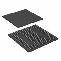
ADSP-BF538BBCZ-4F4 Analog Devices Inc, ADSP-BF538BBCZ-4F4 Datasheet - Page 49

ADSP-BF538BBCZ-4F4
Manufacturer Part Number
ADSP-BF538BBCZ-4F4
Description
IC, FLOAT-PT DSP, 16BIT, 400MHZ, BGA-316
Manufacturer
Analog Devices Inc
Series
Blackfinr
Type
Fixed Pointr
Datasheets
1.ADSP-BF538BBCZ-5F8.pdf
(56 pages)
2.ADSP-BF538BBCZ-4A.pdf
(56 pages)
3.ADSP-BF538BBCZ-4F4.pdf
(60 pages)
Specifications of ADSP-BF538BBCZ-4F4
No. Of Bits
16 Bit
Frequency
400MHz
Supply Voltage
1.2V
Embedded Interface Type
CAN, I2C, PPI, SPI, TWI, UART
No. Of I/o's
54
Flash Memory Size
512KB
Interface
CAN, SPI, SSP, TWI, UART
Clock Rate
400MHz
Non-volatile Memory
FLASH (512 kB)
On-chip Ram
148kB
Voltage - I/o
3.00V, 3.30V
Voltage - Core
1.20V
Operating Temperature
-40°C ~ 85°C
Mounting Type
Surface Mount
Package / Case
316-CSPBGA
Device Core Size
16b
Architecture
Modified Harvard
Format
Fixed Point
Clock Freq (max)
400MHz
Mips
400
Device Input Clock Speed
400MHz
Ram Size
32KB
Program Memory Size
512KB
Operating Supply Voltage (typ)
1.2/2.5/3.3V
Operating Supply Voltage (min)
0.8/2.25/2.7V
Operating Supply Voltage (max)
1.32/3.6V
Operating Temp Range
-40C to 85C
Operating Temperature Classification
Industrial
Mounting
Surface Mount
Pin Count
316
Package Type
CSPBGA
Lead Free Status / RoHS Status
Lead free / RoHS Compliant
For Use With
ADZS-BFAUDIO-EZEXT - BOARD EVAL AUDIO BLACKFIN
Lead Free Status / Rohs Status
Compliant
Example System Hold Time Calculation
To determine the data output hold time in a particular system,
first calculate t
to be the difference between the ADSP-BF538/ADSP-BF538F
processor’s output voltage and the input threshold for the
device requiring the hold time. C
(per data line), and I
(per data line). The hold time will be t
put disable times as specified in the
Page 28
shown in
Capacitive Loading
Output delays and holds are based on standard capacitive loads:
30 pF on all pins (see
(nominal) = 3.0 V/3.3 V.
Page 51
tance. The delay and hold specifications given should be derated
by a factor derived from these figures. The graphs in these fig-
ures may not be linear outside the ranges shown.
V
LOAD
NOTES:
THE WORST CASE TRANSMISSION LINE DELAY IS SHOWN AND CAN BE USED
FOR THE OUTPUT TIMING ANALYSIS TO REFELECT THE TRANSMISSION LINE
EFFECT AND MUST BE CONSIDERED. THE TRANSMISSION LINE (TD) IS FOR
LOAD ONLY AND DOES NOT AFFECT THE DATA SHEET TIMING SPECIFICATIONS.
ANALOG DEVICES RECOMMENDS USING THE IBIS MODEL TIMING FOR A GIVEN
SYSTEM REQUIREMENT. IF NECESSARY, A SYSTEM MAY INCORPORATE
EXTERNAL DRIVERS TO COMPENSATE FOR ANY TIMING DIFFERENCES.
4pF
Figure 44. Equivalent Device Loading for AC Measurements
(Includes All Fixtures)
(for example, t
show how output rise and fall times vary with capaci-
50Ω
Table 27 on Page
70Ω
50Ω
400Ω
2pF
DECAY
using the equation given above. Choose ΔV
L
Figure
is the total leakage or three-state current
DSDAT
45Ω
0.5pF
Figure 45
33).
TESTER PIN ELECTRONICS
for an SDRAM write cycle as
44). V
L
is the total bus capacitance
LOAD
through
ZO = 50Ω (impedance)
TD = 4.04 ± 1.18 ns
Timing Specifications on
DECAY
is 1.5 V for V
T1
plus the various out-
Figure 54 on
Rev. D | Page 49 of 56 | July 2010
DDEXT
OUTPUT
DUT
Figure 45. Typical Rise and Fall Times (10% to 90%) vs. Load Capacitance for
Figure 46. Typical Rise and Fall Times (10% to 90%) vs. Load Capacitance for
14
12
10
12
10
8
6
4
2
0
8
6
4
2
0
0
0
50
50
ADSP-BF538/ADSP-BF538F
Driver A at V
Driver A at V
LOAD CAPACITANCE (pF)
LOAD CAPACITANCE (pF)
100
100
DDEXT
RISE TIME
DDEXT
RISE TIME
= 3.6 V (Max)
= 2.7 V (Min)
150
150
FALL TIME
FALL TIME
200
200
250
250


